MCF5407CAI220 Freescale Semiconductor, MCF5407CAI220 Datasheet - Page 78
MCF5407CAI220
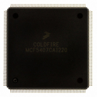
Manufacturer Part Number
MCF5407CAI220
Description
IC MPU 32B 220MHZ COLDF 208-FQFP
Manufacturer
Freescale Semiconductor
Series
MCF540xr
Specifications of MCF5407CAI220
Core Processor
Coldfire V4
Core Size
32-Bit
Speed
220MHz
Connectivity
EBI/EMI, I²C, UART/USART
Peripherals
DMA, WDT
Number Of I /o
16
Program Memory Type
ROMless
Ram Size
4K x 8
Voltage - Supply (vcc/vdd)
1.65 V ~ 3.6 V
Oscillator Type
External
Operating Temperature
-40°C ~ 85°C
Package / Case
208-FQFP
Processor Series
MCF540x
Core
ColdFire V4
Data Bus Width
32 bit
Program Memory Size
8 KB
Data Ram Size
4 KB
Maximum Clock Frequency
162 MHz
Number Of Programmable I/os
16
Operating Supply Voltage
1.8 V to 3.3 V
Mounting Style
SMD/SMT
3rd Party Development Tools
JLINK-CF-BDM26, EWCF
Cpu Speed
220MHz
Embedded Interface Type
I2C, UART
Digital Ic Case Style
FQFP
No. Of Pins
208
Supply Voltage Range
3.3V
Rohs Compliant
Yes
For Use With
M5407C3 - KIT EVAL FOR MCF5407 W/ETHERNET
Lead Free Status / RoHS Status
Lead free / RoHS Compliant
Eeprom Size
-
Program Memory Size
-
Data Converters
-
Lead Free Status / Rohs Status
Lead free / RoHS Compliant
Available stocks
Company
Part Number
Manufacturer
Quantity
Price
Company:

Part Number:
MCF5407CAI220
Manufacturer:
Freescale
Quantity:
789
Company:
Part Number:
MCF5407CAI220
Manufacturer:
Freescale Semiconductor
Quantity:
10 000


Programming Model
2.2.2.2 Vector Base Register (VBR)
The VBR holds the base address of the exception vector table in memory. The displacement
of an exception vector is added to the value in this register to access the vector table.
VBR[19–0] are not implemented and are assumed to be zero, forcing the vector table to be
aligned on a 0-modulo-1-Mbyte boundary.
31 30 29 28 27 26 25 24 23 22 21 20 19 18 17 16 15 14 13 12 11 10 9
8
7
6
5
4
3
2
1
0
Field
Exception vector table base address
—
Reset
0000_0000_0000_0000_0000_0000_0000_0000
R/W Written from a BDM serial command or from the CPU using the MOVEC instruction. VBR can be read from
the debug module only. The upper 12 bits are returned, the low-order 20 bits are undefined.
Rc[11–0]
0x801
Figure 2-6. Vector Base Register (VBR)
2.2.2.3 Cache Control Register (CACR)
The CACR controls operation of both the instruction and data cache memory. It includes
bits for enabling, freezing, and invalidating cache contents. It also includes bits for defining
the default cache mode and write-protect fields. See Section 4.10.1, “Cache Control
Register (CACR).”
2.2.2.4 Access Control Registers (ACR0–ACR3)
The access control registers (ACR0–ACR3) define attributes for four user-defined memory
regions. ACR0 and ACR1 control data memory space and ACR2 and ACR3 control
instruction memory space. Attributes include definition of cache mode, write protect and
buffer write enables. See Section 4.10.2, “Access Control Registers (ACR0–ACR3).”
2.2.2.5 RAM Base Address Registers (RAMBAR0 and RAMBAR1)
The RAMBAR registers determine the base address location of the internal SRAM
modules and indicate the types of references mapped to each. Each RAMBAR includes a
base address, write-protect bit, address space mask bits, and an enable. The RAM base
address must be aligned on a 0-module-2-Kbyte boundary. See Section 4.4.1, “SRAM Base
Address Registers (RAMBAR0/RAMBAR1).”
2.2.2.6 Module Base Address Register (MBAR)
The module base address register (MBAR) defines the logical base address for the
memory-mapped space containing the control registers for the on-chip peripherals. See
Section 6.2.2, “Module Base Address Register (MBAR).”
MCF5407 User’s Manual
2-12
Related parts for MCF5407CAI220
Image
Part Number
Description
Manufacturer
Datasheet
Request
R

Part Number:
Description:
Mcf5407 Coldfire Integrated Microprocessor User
Manufacturer:
Freescale Semiconductor, Inc
Datasheet:
Part Number:
Description:
Manufacturer:
Freescale Semiconductor, Inc
Datasheet:
Part Number:
Description:
Manufacturer:
Freescale Semiconductor, Inc
Datasheet:
Part Number:
Description:
Manufacturer:
Freescale Semiconductor, Inc
Datasheet:
Part Number:
Description:
Manufacturer:
Freescale Semiconductor, Inc
Datasheet:
Part Number:
Description:
Manufacturer:
Freescale Semiconductor, Inc
Datasheet:
Part Number:
Description:
Manufacturer:
Freescale Semiconductor, Inc
Datasheet:
Part Number:
Description:
Manufacturer:
Freescale Semiconductor, Inc
Datasheet:
Part Number:
Description:
Manufacturer:
Freescale Semiconductor, Inc
Datasheet:
Part Number:
Description:
Manufacturer:
Freescale Semiconductor, Inc
Datasheet:
Part Number:
Description:
Manufacturer:
Freescale Semiconductor, Inc
Datasheet:
Part Number:
Description:
Manufacturer:
Freescale Semiconductor, Inc
Datasheet:
Part Number:
Description:
Manufacturer:
Freescale Semiconductor, Inc
Datasheet:
Part Number:
Description:
Manufacturer:
Freescale Semiconductor, Inc
Datasheet:
Part Number:
Description:
Manufacturer:
Freescale Semiconductor, Inc
Datasheet: