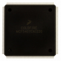
MCF5407CAI220 Freescale Semiconductor, MCF5407CAI220 Datasheet - Page 306

MCF5407CAI220
Manufacturer Part Number
MCF5407CAI220
Description
IC MPU 32B 220MHZ COLDF 208-FQFP
Manufacturer
Freescale Semiconductor
Series
MCF540xr
Specifications of MCF5407CAI220
Core Processor
Coldfire V4
Core Size
32-Bit
Speed
220MHz
Connectivity
EBI/EMI, I²C, UART/USART
Peripherals
DMA, WDT
Number Of I /o
16
Program Memory Type
ROMless
Ram Size
4K x 8
Voltage - Supply (vcc/vdd)
1.65 V ~ 3.6 V
Oscillator Type
External
Operating Temperature
-40°C ~ 85°C
Package / Case
208-FQFP
Processor Series
MCF540x
Core
ColdFire V4
Data Bus Width
32 bit
Program Memory Size
8 KB
Data Ram Size
4 KB
Maximum Clock Frequency
162 MHz
Number Of Programmable I/os
16
Operating Supply Voltage
1.8 V to 3.3 V
Mounting Style
SMD/SMT
3rd Party Development Tools
JLINK-CF-BDM26, EWCF
Cpu Speed
220MHz
Embedded Interface Type
I2C, UART
Digital Ic Case Style
FQFP
No. Of Pins
208
Supply Voltage Range
3.3V
Rohs Compliant
Yes
For Use With
M5407C3 - KIT EVAL FOR MCF5407 W/ETHERNET
Lead Free Status / RoHS Status
Lead free / RoHS Compliant
Eeprom Size
-
Program Memory Size
-
Data Converters
-
Lead Free Status / Rohs Status
Lead free / RoHS Compliant
Available stocks
Company
Part Number
Manufacturer
Quantity
Price
Company:
Part Number:
MCF5407CAI220
Manufacturer:
Freescale
Quantity:
789
Company:
Part Number:
MCF5407CAI220
Manufacturer:
Freescale Semiconductor
Quantity:
10 000
- Current page: 306 of 546
- Download datasheet (7Mb)
SDRAM Example
11.5.5 Mode Register Initialization
When DACR[IMRS] is set, a bus cycle initializes the mode register. If the mode register
setting is read on A[10:0] of the SDRAM on the first bus cycle, the bit settings on the
corresponding MCF5407 address pins must be determined while being aware of masking
requirements.
Table 11-37 lists the desired initialization setting:
Next, this information is mapped to an address to determine the hexadecimal value.
Although A[31:20] corresponds to the address programmed in DACR0, according to how
DACR0 and DMR0 are initialized, bit 19 must be set to hit in the SDRAM. Thus, before
the mode register bit is set, DMR0[19] must be set to enable masking.
11-38
Setting
Setting
(hex)
(hex)
Field
Field
31
15
X
0
Figure 11-29. Mode Register Mapping to MCF5407 A[31:0]
30
14
X
0
MCF5407 Pins
0
0
29
13
X
0
A20
A19
A18
A17
A10
A11
A12
A13
A14
A15
A9
Table 11-37. Mode Register Initialization
28
12
X
0
27
11
X
1
SDRAM Pins
MCF5407 User’s Manual
26
10
X
0
A10
A9
A8
A7
A6
A5
A4
A3
A2
A1
A0
0
8
25
X
0
9
24
X
X
8
Mode Register Initialization
Reserved
Opmode
Opmode
CASL
CASL
CASL
23
WB
X
X
7
BT
BL
BL
BL
22
X
X
6
0
0
21
X
X
5
20
X
X
4
X
0
0
0
0
0
1
0
0
0
0
19
X
0
3
18
X
0
2
0
0
17
X
0
1
16
X
V
X
0
Related parts for MCF5407CAI220
Image
Part Number
Description
Manufacturer
Datasheet
Request
R
Part Number:
Description:
Mcf5407 Coldfire Integrated Microprocessor User
Manufacturer:
Freescale Semiconductor, Inc
Datasheet:
Part Number:
Description:
Manufacturer:
Freescale Semiconductor, Inc
Datasheet:
Part Number:
Description:
Manufacturer:
Freescale Semiconductor, Inc
Datasheet:
Part Number:
Description:
Manufacturer:
Freescale Semiconductor, Inc
Datasheet:
Part Number:
Description:
Manufacturer:
Freescale Semiconductor, Inc
Datasheet:
Part Number:
Description:
Manufacturer:
Freescale Semiconductor, Inc
Datasheet:
Part Number:
Description:
Manufacturer:
Freescale Semiconductor, Inc
Datasheet:
Part Number:
Description:
Manufacturer:
Freescale Semiconductor, Inc
Datasheet:
Part Number:
Description:
Manufacturer:
Freescale Semiconductor, Inc
Datasheet:
Part Number:
Description:
Manufacturer:
Freescale Semiconductor, Inc
Datasheet:
Part Number:
Description:
Manufacturer:
Freescale Semiconductor, Inc
Datasheet:
Part Number:
Description:
Manufacturer:
Freescale Semiconductor, Inc
Datasheet:
Part Number:
Description:
Manufacturer:
Freescale Semiconductor, Inc
Datasheet:
Part Number:
Description:
Manufacturer:
Freescale Semiconductor, Inc
Datasheet:
Part Number:
Description:
Manufacturer:
Freescale Semiconductor, Inc
Datasheet:


