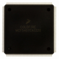
MCF5407CAI220 Freescale Semiconductor, MCF5407CAI220 Datasheet - Page 60

MCF5407CAI220
Manufacturer Part Number
MCF5407CAI220
Description
IC MPU 32B 220MHZ COLDF 208-FQFP
Manufacturer
Freescale Semiconductor
Series
MCF540xr
Specifications of MCF5407CAI220
Core Processor
Coldfire V4
Core Size
32-Bit
Speed
220MHz
Connectivity
EBI/EMI, I²C, UART/USART
Peripherals
DMA, WDT
Number Of I /o
16
Program Memory Type
ROMless
Ram Size
4K x 8
Voltage - Supply (vcc/vdd)
1.65 V ~ 3.6 V
Oscillator Type
External
Operating Temperature
-40°C ~ 85°C
Package / Case
208-FQFP
Processor Series
MCF540x
Core
ColdFire V4
Data Bus Width
32 bit
Program Memory Size
8 KB
Data Ram Size
4 KB
Maximum Clock Frequency
162 MHz
Number Of Programmable I/os
16
Operating Supply Voltage
1.8 V to 3.3 V
Mounting Style
SMD/SMT
3rd Party Development Tools
JLINK-CF-BDM26, EWCF
Cpu Speed
220MHz
Embedded Interface Type
I2C, UART
Digital Ic Case Style
FQFP
No. Of Pins
208
Supply Voltage Range
3.3V
Rohs Compliant
Yes
For Use With
M5407C3 - KIT EVAL FOR MCF5407 W/ETHERNET
Lead Free Status / RoHS Status
Lead free / RoHS Compliant
Eeprom Size
-
Program Memory Size
-
Data Converters
-
Lead Free Status / Rohs Status
Lead free / RoHS Compliant
Available stocks
Company
Part Number
Manufacturer
Quantity
Price
Company:
Part Number:
MCF5407CAI220
Manufacturer:
Freescale
Quantity:
789
Company:
Part Number:
MCF5407CAI220
Manufacturer:
Freescale Semiconductor
Quantity:
10 000
- Current page: 60 of 546
- Download datasheet (7Mb)
Status register (SR)
Vector base register
(VBR)
Cache configuration
register (CACR)
Access control
registers (ACR0/1,
ACR2/3)
RAM base address
registers (RAMBAR0,
RAMBAR1)
Module base address
register (MBAR)
Programming Model, Addressing Modes, and Instruction Set
1.4.3 Supervisor Registers
Table 1-2 summarizes the MCF5407 supervisor-level registers.
1.4.4 Instruction Set
The Version 4 ColdFire core implements Revision B of the instruction set, which adds
opcodes to enhance support for byte- and word-sized operands and position-independent
code. The ColdFire instruction set supports high-level languages and is optimized for those
instructions most commonly generated by compilers in embedded applications. Table 2-8
provides an alphabetized listing of the ColdFire instruction set opcodes, supported
Program counter
(PC)
Condition code
register (CCR)
MAC status
register (MACSR)
Accumulator
(ACC)
Mask register
(MASK)
1-16
Register
Register
Contains the address of the instruction currently being executed by the MCF5407 processor
The CCR is the lower byte of the SR. It contains indicator flags that reflect the result of a previous
operation and are used for conditional instruction execution.
Defines the operating configuration of the MAC unit and contains indicator flags from the results
of MAC instructions.
General-purpose register used to accumulate the results of MAC operations
General-purpose register provides an optional address mask for MAC instructions that fetch
operands from memory. It is useful in the implementation of circular queues in operand memory.
The upper byte of the SR provides interrupt information in addition to a variety of mode indicators
signaling the operating state of the ColdFire processor. The lower byte of the SR is the CCR, as
shown in Figure 1-4.
Defines the upper 12 bits of the base address of the exception vector table used during exception
processing. The low-order 20 bits are forced to zero, locating the vector table on 0-modulo-1
Mbyte address.
Defines the operating modes of the Version 4 cache memories. Control fields configuring the
instruction, data, and branch cache are provided by this register, along with the default attributes
for the 4-Gbyte address space.
Define address ranges and attributes associated with various memory regions within the 4-Gbyte
address space. Each ACR defines the location of a given memory region and assigns attributes
such as write-protection and cache mode (copyback, write-through, cacheability). ACR0 and
ACR1 support data memory; ACR2 and ACR3 support instruction memory. Additionally, CACR
fields assign default attributes to the instruction and data memory spaces.
Provide the logical base address for the two 2-Kbyte SRAM modules and define attributes and
access types allowed for the corresponding SRAM.
Defines the logical base address for the memory-mapped space containing the control registers
for the on-chip peripherals.
Table 1-1. User-Level Registers (Continued)
Table 1-2. Supervisor-Level Registers
MCF5407 User’s Manual
Description
Description
Related parts for MCF5407CAI220
Image
Part Number
Description
Manufacturer
Datasheet
Request
R
Part Number:
Description:
Mcf5407 Coldfire Integrated Microprocessor User
Manufacturer:
Freescale Semiconductor, Inc
Datasheet:
Part Number:
Description:
Manufacturer:
Freescale Semiconductor, Inc
Datasheet:
Part Number:
Description:
Manufacturer:
Freescale Semiconductor, Inc
Datasheet:
Part Number:
Description:
Manufacturer:
Freescale Semiconductor, Inc
Datasheet:
Part Number:
Description:
Manufacturer:
Freescale Semiconductor, Inc
Datasheet:
Part Number:
Description:
Manufacturer:
Freescale Semiconductor, Inc
Datasheet:
Part Number:
Description:
Manufacturer:
Freescale Semiconductor, Inc
Datasheet:
Part Number:
Description:
Manufacturer:
Freescale Semiconductor, Inc
Datasheet:
Part Number:
Description:
Manufacturer:
Freescale Semiconductor, Inc
Datasheet:
Part Number:
Description:
Manufacturer:
Freescale Semiconductor, Inc
Datasheet:
Part Number:
Description:
Manufacturer:
Freescale Semiconductor, Inc
Datasheet:
Part Number:
Description:
Manufacturer:
Freescale Semiconductor, Inc
Datasheet:
Part Number:
Description:
Manufacturer:
Freescale Semiconductor, Inc
Datasheet:
Part Number:
Description:
Manufacturer:
Freescale Semiconductor, Inc
Datasheet:
Part Number:
Description:
Manufacturer:
Freescale Semiconductor, Inc
Datasheet:


