MCF5407CAI220 Freescale Semiconductor, MCF5407CAI220 Datasheet - Page 240
MCF5407CAI220
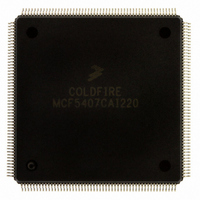
Manufacturer Part Number
MCF5407CAI220
Description
IC MPU 32B 220MHZ COLDF 208-FQFP
Manufacturer
Freescale Semiconductor
Series
MCF540xr
Specifications of MCF5407CAI220
Core Processor
Coldfire V4
Core Size
32-Bit
Speed
220MHz
Connectivity
EBI/EMI, I²C, UART/USART
Peripherals
DMA, WDT
Number Of I /o
16
Program Memory Type
ROMless
Ram Size
4K x 8
Voltage - Supply (vcc/vdd)
1.65 V ~ 3.6 V
Oscillator Type
External
Operating Temperature
-40°C ~ 85°C
Package / Case
208-FQFP
Processor Series
MCF540x
Core
ColdFire V4
Data Bus Width
32 bit
Program Memory Size
8 KB
Data Ram Size
4 KB
Maximum Clock Frequency
162 MHz
Number Of Programmable I/os
16
Operating Supply Voltage
1.8 V to 3.3 V
Mounting Style
SMD/SMT
3rd Party Development Tools
JLINK-CF-BDM26, EWCF
Cpu Speed
220MHz
Embedded Interface Type
I2C, UART
Digital Ic Case Style
FQFP
No. Of Pins
208
Supply Voltage Range
3.3V
Rohs Compliant
Yes
For Use With
M5407C3 - KIT EVAL FOR MCF5407 W/ETHERNET
Lead Free Status / RoHS Status
Lead free / RoHS Compliant
Eeprom Size
-
Program Memory Size
-
Data Converters
-
Lead Free Status / Rohs Status
Lead free / RoHS Compliant
Available stocks
Company
Part Number
Manufacturer
Quantity
Price
Company:

Part Number:
MCF5407CAI220
Manufacturer:
Freescale
Quantity:
789
Company:
Part Number:
MCF5407CAI220
Manufacturer:
Freescale Semiconductor
Quantity:
10 000


I
Instead of signalling a STOP, the master can repeat the START signal, followed by a calling
command, (A in Figure 8-3). A repeated START occurs when a START signal is generated
without first generating a STOP signal to end the communication.
The master uses a repeated START to communicate with another slave or with the same
slave in a different mode (transmit/receive mode) without releasing the bus.
8.4.1 Arbitration Procedure
If multiple devices simultaneously request the bus, the bus clock is determined by a
8-4
2
C Protocol
SCL
SDA
3. Data transfer—When successful slave addressing is achieved, the data transfer can
4. STOP signal—The master can terminate communication by generating a STOP
START
Signal
Each slave must have a unique address. An I
that is the same as its slave address; it cannot be master and slave at the same time.
The slave whose address matches that sent by the master pulls SDA low at the ninth
clock (D) to return an acknowledge bit.
proceed (E) on a byte-by-byte basis in the direction specified by the R/W bit sent by
the calling master.
Data can be changed only while SCL is low and must be held stable while SCL is
high, as Figure 8-2 shows. SCL is pulsed once for each data bit, with the msb being
sent first. The receiving device must acknowledge each byte by pulling SDA low at
the ninth clock; therefore, a data byte transfer takes nine clock pulses.
If it does not acknowledge the master, the slave receiver must leave SDA high. The
master can then generate a STOP signal to abort the data transfer or generate a
START signal (repeated start, shown in Figure 8-3) to start a new calling sequence.
If the master receiver does not acknowledge the slave transmitter after a byte
transmission, it means end-of-data to the slave. The slave releases SDA for the
master to generate a STOP or START signal.
signal to free the bus. A STOP signal is defined as a low-to-high transition of SDA
while SCL is at logical high (F). Note that a master can generate a STOP even if the
slave has made an acknowledgment, at which point the slave must release the bus.
AD7 AD6 AD5 AD4 AD3 AD2 AD1 R/W
msb
1
2
Calling Address
3
4
5
6
Figure 8-3. Repeated START
7
R/W
lsb
MCF5407 User’s Manual
8
ACK
Bit
9
XX
Repeated
START
Signal
AD7 AD6 AD5 AD4 AD3 AD2 AD1 R/W
msb
A
1
2
C master must not transmit an address
2
New Calling Address
Stop
3
4
5
6
7
R/W No
lsb
8
ACK
Bit
9
STOP
Signal
Related parts for MCF5407CAI220
Image
Part Number
Description
Manufacturer
Datasheet
Request
R

Part Number:
Description:
Mcf5407 Coldfire Integrated Microprocessor User
Manufacturer:
Freescale Semiconductor, Inc
Datasheet:
Part Number:
Description:
Manufacturer:
Freescale Semiconductor, Inc
Datasheet:
Part Number:
Description:
Manufacturer:
Freescale Semiconductor, Inc
Datasheet:
Part Number:
Description:
Manufacturer:
Freescale Semiconductor, Inc
Datasheet:
Part Number:
Description:
Manufacturer:
Freescale Semiconductor, Inc
Datasheet:
Part Number:
Description:
Manufacturer:
Freescale Semiconductor, Inc
Datasheet:
Part Number:
Description:
Manufacturer:
Freescale Semiconductor, Inc
Datasheet:
Part Number:
Description:
Manufacturer:
Freescale Semiconductor, Inc
Datasheet:
Part Number:
Description:
Manufacturer:
Freescale Semiconductor, Inc
Datasheet:
Part Number:
Description:
Manufacturer:
Freescale Semiconductor, Inc
Datasheet:
Part Number:
Description:
Manufacturer:
Freescale Semiconductor, Inc
Datasheet:
Part Number:
Description:
Manufacturer:
Freescale Semiconductor, Inc
Datasheet:
Part Number:
Description:
Manufacturer:
Freescale Semiconductor, Inc
Datasheet:
Part Number:
Description:
Manufacturer:
Freescale Semiconductor, Inc
Datasheet:
Part Number:
Description:
Manufacturer:
Freescale Semiconductor, Inc
Datasheet: