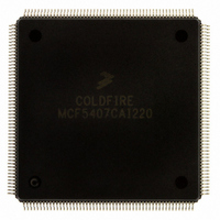
MCF5407CAI220 Freescale Semiconductor, MCF5407CAI220 Datasheet - Page 284

MCF5407CAI220
Manufacturer Part Number
MCF5407CAI220
Description
IC MPU 32B 220MHZ COLDF 208-FQFP
Manufacturer
Freescale Semiconductor
Series
MCF540xr
Specifications of MCF5407CAI220
Core Processor
Coldfire V4
Core Size
32-Bit
Speed
220MHz
Connectivity
EBI/EMI, I²C, UART/USART
Peripherals
DMA, WDT
Number Of I /o
16
Program Memory Type
ROMless
Ram Size
4K x 8
Voltage - Supply (vcc/vdd)
1.65 V ~ 3.6 V
Oscillator Type
External
Operating Temperature
-40°C ~ 85°C
Package / Case
208-FQFP
Processor Series
MCF540x
Core
ColdFire V4
Data Bus Width
32 bit
Program Memory Size
8 KB
Data Ram Size
4 KB
Maximum Clock Frequency
162 MHz
Number Of Programmable I/os
16
Operating Supply Voltage
1.8 V to 3.3 V
Mounting Style
SMD/SMT
3rd Party Development Tools
JLINK-CF-BDM26, EWCF
Cpu Speed
220MHz
Embedded Interface Type
I2C, UART
Digital Ic Case Style
FQFP
No. Of Pins
208
Supply Voltage Range
3.3V
Rohs Compliant
Yes
For Use With
M5407C3 - KIT EVAL FOR MCF5407 W/ETHERNET
Lead Free Status / RoHS Status
Lead free / RoHS Compliant
Eeprom Size
-
Program Memory Size
-
Data Converters
-
Lead Free Status / Rohs Status
Lead free / RoHS Compliant
Available stocks
Company
Part Number
Manufacturer
Quantity
Price
Company:
Part Number:
MCF5407CAI220
Manufacturer:
Freescale
Quantity:
789
Company:
Part Number:
MCF5407CAI220
Manufacturer:
Freescale Semiconductor
Quantity:
10 000
- Current page: 284 of 546
- Download datasheet (7Mb)
Synchronous Operation
11.3.3.5 Refresh Operation
The DRAM controller supports CAS-before-RAS refresh operations that are not
synchronized to bus activity. A special DRAMW pin is provided so refresh can occur
regardless of the state of the processor bus.
When the refresh counter rolls over, it sets an internal flag to indicate that a refresh is
pending. If that happens during a continuous page-mode access, the page is closed (RAS
precharged) when the data transfer completes to allow the refresh to occur. The flag is
cleared when the refresh cycle is run. Both memory blocks are simultaneously refreshed as
determined by the DCR. DRAM accesses are delayed during refresh. Only an active bus
access to a DRAM block can delay refresh.
Figure 11-12 shows a bus cycle delayed by a refresh operation. Notice that DRAMW is
forced high during refresh. The row address is held until the pending DRAM access.
CLKIN
A[31:0]
RRP = 01
RAS[1] or [0]
RRA = 01
CAS[3:0]
DRAMW
Refresh
Access
Figure 11-12. DRAM Access Delayed by Refresh
11.4 Synchronous Operation
By running synchronously with the system clock instead of responding to asynchronous
control signals, SDRAM can (after an initial latency period) be accessed on every clock;
5-1-1-1 is a typical MCF5407 burst rate to SDRAM.
Note that because the MCF5407 cannot have more than one page open at a time, it does not
support interleaving.
SDRAM controllers are more sophisticated than asynchronous DRAM controllers. Not
only must they manage addresses and data, but they must send special commands for such
functions as precharge, read, write, burst, auto-refresh, and various combinations of these
functions. Table 11-10 lists common SDRAM commands.
MCF5407 User’s Manual
11-16
Related parts for MCF5407CAI220
Image
Part Number
Description
Manufacturer
Datasheet
Request
R
Part Number:
Description:
Mcf5407 Coldfire Integrated Microprocessor User
Manufacturer:
Freescale Semiconductor, Inc
Datasheet:
Part Number:
Description:
Manufacturer:
Freescale Semiconductor, Inc
Datasheet:
Part Number:
Description:
Manufacturer:
Freescale Semiconductor, Inc
Datasheet:
Part Number:
Description:
Manufacturer:
Freescale Semiconductor, Inc
Datasheet:
Part Number:
Description:
Manufacturer:
Freescale Semiconductor, Inc
Datasheet:
Part Number:
Description:
Manufacturer:
Freescale Semiconductor, Inc
Datasheet:
Part Number:
Description:
Manufacturer:
Freescale Semiconductor, Inc
Datasheet:
Part Number:
Description:
Manufacturer:
Freescale Semiconductor, Inc
Datasheet:
Part Number:
Description:
Manufacturer:
Freescale Semiconductor, Inc
Datasheet:
Part Number:
Description:
Manufacturer:
Freescale Semiconductor, Inc
Datasheet:
Part Number:
Description:
Manufacturer:
Freescale Semiconductor, Inc
Datasheet:
Part Number:
Description:
Manufacturer:
Freescale Semiconductor, Inc
Datasheet:
Part Number:
Description:
Manufacturer:
Freescale Semiconductor, Inc
Datasheet:
Part Number:
Description:
Manufacturer:
Freescale Semiconductor, Inc
Datasheet:
Part Number:
Description:
Manufacturer:
Freescale Semiconductor, Inc
Datasheet:


