MCF5407CAI220 Freescale Semiconductor, MCF5407CAI220 Datasheet - Page 319
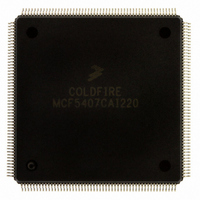
MCF5407CAI220
Manufacturer Part Number
MCF5407CAI220
Description
IC MPU 32B 220MHZ COLDF 208-FQFP
Manufacturer
Freescale Semiconductor
Series
MCF540xr
Specifications of MCF5407CAI220
Core Processor
Coldfire V4
Core Size
32-Bit
Speed
220MHz
Connectivity
EBI/EMI, I²C, UART/USART
Peripherals
DMA, WDT
Number Of I /o
16
Program Memory Type
ROMless
Ram Size
4K x 8
Voltage - Supply (vcc/vdd)
1.65 V ~ 3.6 V
Oscillator Type
External
Operating Temperature
-40°C ~ 85°C
Package / Case
208-FQFP
Processor Series
MCF540x
Core
ColdFire V4
Data Bus Width
32 bit
Program Memory Size
8 KB
Data Ram Size
4 KB
Maximum Clock Frequency
162 MHz
Number Of Programmable I/os
16
Operating Supply Voltage
1.8 V to 3.3 V
Mounting Style
SMD/SMT
3rd Party Development Tools
JLINK-CF-BDM26, EWCF
Cpu Speed
220MHz
Embedded Interface Type
I2C, UART
Digital Ic Case Style
FQFP
No. Of Pins
208
Supply Voltage Range
3.3V
Rohs Compliant
Yes
For Use With
M5407C3 - KIT EVAL FOR MCF5407 W/ETHERNET
Lead Free Status / RoHS Status
Lead free / RoHS Compliant
Eeprom Size
-
Program Memory Size
-
Data Converters
-
Lead Free Status / Rohs Status
Lead free / RoHS Compliant
Available stocks
Company
Part Number
Manufacturer
Quantity
Price
Company:

Part Number:
MCF5407CAI220
Manufacturer:
Freescale
Quantity:
789
Company:
Part Number:
MCF5407CAI220
Manufacturer:
Freescale Semiconductor
Quantity:
10 000


12.4.1 Source Address Registers (SAR0–SAR3)
SARn, Figure 12-5, contains the address from which the DMA controller requests data. In
single-address mode, SARn provides the address regardless of the direction.
12.4.2 Destination Address Registers (DAR0–DAR3)
For dual-address transfers only, DARn, Figure 12-6, holds the address to which the DMA
controller sends data.
12.4.3 Byte Count Registers (BCR0–BCR3)
BCRn, Figure 12-7, holds the number of bytes yet to be transferred for a given block. BCRn
decrements on the successful completion of the address transfer of either a write transfer in
dual-address mode or any transfer in single-address mode. BCRn decrements by 1, 2, 4, or
16 for byte, word, longword, or line accesses, respectively.
Address
Address
Reset
Reset
Field
Field
R/W
R/W
31
31
SAR/DAR address ranges cannot be programmed to on-chip
SRAM because it cannot be accessed by on-chip DMA.
On-chip DMAs do not maintain coherency with MCF5407
caches and so must not transfer data to cacheable memory.
Figure 12-6. Destination Address Registers (DARn)
Figure 12-5. Source Address Registers (SARn)
Chapter 12. DMA Controller Module
0000_0000_0000_0000_0000_0000_0000_0000
0000_0000_0000_0000_0000_0000_0000_0000
MBAR + 0x300, 0x340, 0x380, 0x3C0
MBAR + 304, 0x344, 0x384, 0x3C4
NOTE:
NOTE:
SAR
DAR
R/W
R/W
DMA Controller Module Programming Model
12-7
0
0
Related parts for MCF5407CAI220
Image
Part Number
Description
Manufacturer
Datasheet
Request
R

Part Number:
Description:
Mcf5407 Coldfire Integrated Microprocessor User
Manufacturer:
Freescale Semiconductor, Inc
Datasheet:
Part Number:
Description:
Manufacturer:
Freescale Semiconductor, Inc
Datasheet:
Part Number:
Description:
Manufacturer:
Freescale Semiconductor, Inc
Datasheet:
Part Number:
Description:
Manufacturer:
Freescale Semiconductor, Inc
Datasheet:
Part Number:
Description:
Manufacturer:
Freescale Semiconductor, Inc
Datasheet:
Part Number:
Description:
Manufacturer:
Freescale Semiconductor, Inc
Datasheet:
Part Number:
Description:
Manufacturer:
Freescale Semiconductor, Inc
Datasheet:
Part Number:
Description:
Manufacturer:
Freescale Semiconductor, Inc
Datasheet:
Part Number:
Description:
Manufacturer:
Freescale Semiconductor, Inc
Datasheet:
Part Number:
Description:
Manufacturer:
Freescale Semiconductor, Inc
Datasheet:
Part Number:
Description:
Manufacturer:
Freescale Semiconductor, Inc
Datasheet:
Part Number:
Description:
Manufacturer:
Freescale Semiconductor, Inc
Datasheet:
Part Number:
Description:
Manufacturer:
Freescale Semiconductor, Inc
Datasheet:
Part Number:
Description:
Manufacturer:
Freescale Semiconductor, Inc
Datasheet:
Part Number:
Description:
Manufacturer:
Freescale Semiconductor, Inc
Datasheet: