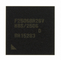
DF2506BR26DV Renesas Electronics America, DF2506BR26DV Datasheet - Page 125

DF2506BR26DV
Manufacturer Part Number
DF2506BR26DV
Description
IC H8S/2506 MCU FLASH 176-LFBGA
Manufacturer
Renesas Electronics America
Series
H8® H8S/2500r
Specifications of DF2506BR26DV
Core Processor
H8S/2000
Core Size
16-Bit
Speed
26MHz
Connectivity
I²C, SCI
Peripherals
POR, PWM, WDT
Number Of I /o
104
Program Memory Size
512KB (512K x 8)
Program Memory Type
FLASH
Ram Size
32K x 8
Voltage - Supply (vcc/vdd)
3 V ~ 5.5 V
Data Converters
A/D 16x10b; D/A 2x8b
Oscillator Type
Internal
Operating Temperature
-40°C ~ 85°C
Package / Case
176-LFBGA
Lead Free Status / RoHS Status
Lead free / RoHS Compliant
Eeprom Size
-
Available stocks
Company
Part Number
Manufacturer
Quantity
Price
Company:
Part Number:
DF2506BR26DV
Manufacturer:
Renesas Electronics America
Quantity:
10 000
- Current page: 125 of 980
- Download datasheet (6Mb)
4.3
A reset has the highest exception priority.
When the RES or MRES pin goes low, all processing halts and this LSI enters the reset state. A
reset initializes the internal state of the CPU and the registers of the on-chip peripheral modules.
This LSI enters interrupt control mode 0 immediately after a reset.
When the RES or MRES pin goes high from the low state, this LSI starts reset exception handling.
The chip can also be reset by overflow of the watchdog timer. For details, see section 12,
Watchdog Timer (WDT).
4.3.1
The LSI supports two types of resets: power-on reset and manual reset.
Table 4.3 shows the types of reset. Set to power-on reset when the power is tuned on.
The CPU internal status is initialized both by the power-on reset and the manual reset. By a
power-on reset, all registers of the on-chip peripheral modules are initialized; by a manual reset,
registers of the on-chip peripheral modules, except for the bus controller and I/O ports, are
initialized. The status of the bus controller and I/O ports is maintained.
By a manual reset, on-chip peripheral modules are initialized and thus ports used as input/output
pins of the on-chip peripheral modules are switched to input/output ports controlled by DDR and
DR.
Table 4.3
Legend:
*:
The power-on reset and the manual reset are also available for the reset by the watchdog timer.
To enable the MRES pin, set the MRESE bit in SYSCR to 1.
Types
Power-on reset
Manual reset
Don’t care
Reset
Types of Reset
Types of Reset
Reset Shift Conditions
MRES
*
Low
RES
Low
High
Internal State
CPU
Initialized
Initialized
On-Chip Peripheral Modules
Initialized
Initialized except for bus controller
and I/O ports
Rev. 6.00 Sep. 24, 2009 Page 77 of 928
Section 4 Exception Handling
REJ09B0099-0600
Related parts for DF2506BR26DV
Image
Part Number
Description
Manufacturer
Datasheet
Request
R

Part Number:
Description:
KIT STARTER FOR M16C/29
Manufacturer:
Renesas Electronics America
Datasheet:

Part Number:
Description:
KIT STARTER FOR R8C/2D
Manufacturer:
Renesas Electronics America
Datasheet:

Part Number:
Description:
R0K33062P STARTER KIT
Manufacturer:
Renesas Electronics America
Datasheet:

Part Number:
Description:
KIT STARTER FOR R8C/23 E8A
Manufacturer:
Renesas Electronics America
Datasheet:

Part Number:
Description:
KIT STARTER FOR R8C/25
Manufacturer:
Renesas Electronics America
Datasheet:

Part Number:
Description:
KIT STARTER H8S2456 SHARPE DSPLY
Manufacturer:
Renesas Electronics America
Datasheet:

Part Number:
Description:
KIT STARTER FOR R8C38C
Manufacturer:
Renesas Electronics America
Datasheet:

Part Number:
Description:
KIT STARTER FOR R8C35C
Manufacturer:
Renesas Electronics America
Datasheet:

Part Number:
Description:
KIT STARTER FOR R8CL3AC+LCD APPS
Manufacturer:
Renesas Electronics America
Datasheet:

Part Number:
Description:
KIT STARTER FOR RX610
Manufacturer:
Renesas Electronics America
Datasheet:

Part Number:
Description:
KIT STARTER FOR R32C/118
Manufacturer:
Renesas Electronics America
Datasheet:

Part Number:
Description:
KIT DEV RSK-R8C/26-29
Manufacturer:
Renesas Electronics America
Datasheet:

Part Number:
Description:
KIT STARTER FOR SH7124
Manufacturer:
Renesas Electronics America
Datasheet:

Part Number:
Description:
KIT STARTER FOR H8SX/1622
Manufacturer:
Renesas Electronics America
Datasheet:

Part Number:
Description:
KIT DEV FOR SH7203
Manufacturer:
Renesas Electronics America
Datasheet:


