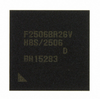
DF2506BR26DV Renesas Electronics America, DF2506BR26DV Datasheet - Page 785

DF2506BR26DV
Manufacturer Part Number
DF2506BR26DV
Description
IC H8S/2506 MCU FLASH 176-LFBGA
Manufacturer
Renesas Electronics America
Series
H8® H8S/2500r
Specifications of DF2506BR26DV
Core Processor
H8S/2000
Core Size
16-Bit
Speed
26MHz
Connectivity
I²C, SCI
Peripherals
POR, PWM, WDT
Number Of I /o
104
Program Memory Size
512KB (512K x 8)
Program Memory Type
FLASH
Ram Size
32K x 8
Voltage - Supply (vcc/vdd)
3 V ~ 5.5 V
Data Converters
A/D 16x10b; D/A 2x8b
Oscillator Type
Internal
Operating Temperature
-40°C ~ 85°C
Package / Case
176-LFBGA
Lead Free Status / RoHS Status
Lead free / RoHS Compliant
Eeprom Size
-
Available stocks
Company
Part Number
Manufacturer
Quantity
Price
Company:
Part Number:
DF2506BR26DV
Manufacturer:
Renesas Electronics America
Quantity:
10 000
- Current page: 785 of 980
- Download datasheet (6Mb)
Table 20.13 Each Command in Programmer Mode
20.9.3
1. On completion of an automatic program, automatic erase, or status read, the LSI enters a
2. In memory-read mode, command programming can be performed as in the case of command
3. Continuous read can be performed after the transition to memory-read mode is made.
4. Transition to the memory-read mode is made after power has been supplied.
Notes: 1.
Command
Name
Memory-read
mode
Auto- program
mode
Auto-erase
mode
Status-read
mode
command waiting state. To read the contents of memory after these operations, issue the
command to change the mode to memory-read mode before reading from the memory.
waiting state.
For the AC characteristics in memory-read mode, see section 20.11, AC Characteristics and
Timing in Programmer Mode.
2.
Memory-Read Mode
In automatic programming mode, 129 cycles of command programming are required
because of simultaneous 128-byte programming.
In memory-read mode, the number of cycles varies according to the number of
address writing cycles (n).
Cycle
Count
1 + n
129
2
2
Target
Memory
MAT
User MAT
User boot
MAT
User MAT
User boot
MAT
User MAT
User boot
MAT
Common to
both MAT
Mode
write
write
write
write
write
write
write
First Cycle
Address
X
X
X
X
X
X
X
Rev. 6.00 Sep. 24, 2009 Page 737 of 928
Data
H'00
H'05
H'40
H'45
H'20
H'25
H'71
Mode
read
write
write
write
Section 20 Flash Memory
Second Cycle
Address
RA
WA
X
X
REJ09B0099-0600
Data
Dout
Din
H'20
H'71
Related parts for DF2506BR26DV
Image
Part Number
Description
Manufacturer
Datasheet
Request
R

Part Number:
Description:
KIT STARTER FOR M16C/29
Manufacturer:
Renesas Electronics America
Datasheet:

Part Number:
Description:
KIT STARTER FOR R8C/2D
Manufacturer:
Renesas Electronics America
Datasheet:

Part Number:
Description:
R0K33062P STARTER KIT
Manufacturer:
Renesas Electronics America
Datasheet:

Part Number:
Description:
KIT STARTER FOR R8C/23 E8A
Manufacturer:
Renesas Electronics America
Datasheet:

Part Number:
Description:
KIT STARTER FOR R8C/25
Manufacturer:
Renesas Electronics America
Datasheet:

Part Number:
Description:
KIT STARTER H8S2456 SHARPE DSPLY
Manufacturer:
Renesas Electronics America
Datasheet:

Part Number:
Description:
KIT STARTER FOR R8C38C
Manufacturer:
Renesas Electronics America
Datasheet:

Part Number:
Description:
KIT STARTER FOR R8C35C
Manufacturer:
Renesas Electronics America
Datasheet:

Part Number:
Description:
KIT STARTER FOR R8CL3AC+LCD APPS
Manufacturer:
Renesas Electronics America
Datasheet:

Part Number:
Description:
KIT STARTER FOR RX610
Manufacturer:
Renesas Electronics America
Datasheet:

Part Number:
Description:
KIT STARTER FOR R32C/118
Manufacturer:
Renesas Electronics America
Datasheet:

Part Number:
Description:
KIT DEV RSK-R8C/26-29
Manufacturer:
Renesas Electronics America
Datasheet:

Part Number:
Description:
KIT STARTER FOR SH7124
Manufacturer:
Renesas Electronics America
Datasheet:

Part Number:
Description:
KIT STARTER FOR H8SX/1622
Manufacturer:
Renesas Electronics America
Datasheet:

Part Number:
Description:
KIT DEV FOR SH7203
Manufacturer:
Renesas Electronics America
Datasheet:


