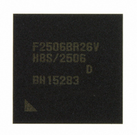
DF2506BR26DV Renesas Electronics America, DF2506BR26DV Datasheet - Page 943

DF2506BR26DV
Manufacturer Part Number
DF2506BR26DV
Description
IC H8S/2506 MCU FLASH 176-LFBGA
Manufacturer
Renesas Electronics America
Series
H8® H8S/2500r
Specifications of DF2506BR26DV
Core Processor
H8S/2000
Core Size
16-Bit
Speed
26MHz
Connectivity
I²C, SCI
Peripherals
POR, PWM, WDT
Number Of I /o
104
Program Memory Size
512KB (512K x 8)
Program Memory Type
FLASH
Ram Size
32K x 8
Voltage - Supply (vcc/vdd)
3 V ~ 5.5 V
Data Converters
A/D 16x10b; D/A 2x8b
Oscillator Type
Internal
Operating Temperature
-40°C ~ 85°C
Package / Case
176-LFBGA
Lead Free Status / RoHS Status
Lead free / RoHS Compliant
Eeprom Size
-
Available stocks
Company
Part Number
Manufacturer
Quantity
Price
Company:
Part Number:
DF2506BR26DV
Manufacturer:
Renesas Electronics America
Quantity:
10 000
- Current page: 943 of 980
- Download datasheet (6Mb)
24.4.5
Table 24.9 lists the timing of on-chip peripheral modules. Table 24.10 lists the I
Table 24.9 Timing of On-Chip Peripheral Modules
Condition A
V
3.3 V ± 0.3 V (BUFGC1 and BUFGC2 in ICPCR are 1),
AV
8 to 26 MHz, T
specifications)
Condition B
V
3.3 V ± 0.3 V (BUFGC1 and BUFGC2 in ICPCR are 1),
AV
8 to 20 MHz, Ta = –40°C to +85°C (wide-range specifications)
Item
I/O ports
*
TPU
TMR
WDT_1
3
CC
CC
CC
CC
= P1V
= P1V
= 3.0 V to 5.5 V, V
= 3.0 V to 5.5 V, V
Timing of On-Chip Peripheral Modules
CC
CC
Output data delay time
Input data setup time
Input data hold time
Timer output delay time
Timer input setup time
Timer clock input setup time
Timer clock
pulse width
Timer output delay time
Timer reset input setup time
Timer clock input setup time
Timer clock
pulse width
BUZZ output delay time
= P2V
= P2V
a
= –20°C to +75°C (regular specifications)*
(for H8S/2552 Group, H8S/2506 Group):
(for H8S/2556 Group):
CC
CC
= 5.0 V ± 0.5 V (BUFGC1 and BUFGC2 in ICPCR are 0)/
= 5.0 V ± 0.5 V (BUFGC1 and BUFGC2 in ICPCR are 0)/
ref
ref
Single edge
Both edges
Single edge
Both edges
= 3.0 V to AV
= 3.0 V to AV
Symbol Min.
t
t
t
t
t
t
t
t
t
t
t
t
t
t
PWD
PRS
PRH
TOCD
TICS
TCKS
TCKWH
TCKWL
TMOD
TMRS
TMCS
TMCWH
TMCWL
BUZD
CC
CC
, V
, V
SS
SS
= AV
= AV
⎯
28
28
⎯
28
28
1.5
2.5
⎯
28
28
1.5
2.5
⎯
Condition A
SS
SS
= 0 V, φ= 32.768 kHz,
= 0 V, φ= 32.768 kHz,
Max.
38
⎯
⎯
38
⎯
⎯
⎯
⎯
38
⎯
⎯
⎯
⎯
38
1
, T
Rev. 6.00 Sep. 24, 2009 Page 895 of 928
a
= –40°C to +85°C (wide-range
Min.
⎯
30
30
⎯
30
30
1.5
2.5
⎯
30
30
1.5
2.5
⎯
Section 24 Electrical Characteristics
Condition B
Max.
50
⎯
⎯
50
⎯
⎯
⎯
⎯
50
⎯
⎯
⎯
⎯
50
2
Unit
ns
ns
ns
t
ns
ns
ns
t
ns
C2 bus timing.
cyc
cyc
REJ09B0099-0600
Test
Conditions
Figure 24.14
Figure 24.15
Figure 24.16
Figure 24.17
Figure 24.19
Figure 24.18
Figure 24.20
Related parts for DF2506BR26DV
Image
Part Number
Description
Manufacturer
Datasheet
Request
R

Part Number:
Description:
KIT STARTER FOR M16C/29
Manufacturer:
Renesas Electronics America
Datasheet:

Part Number:
Description:
KIT STARTER FOR R8C/2D
Manufacturer:
Renesas Electronics America
Datasheet:

Part Number:
Description:
R0K33062P STARTER KIT
Manufacturer:
Renesas Electronics America
Datasheet:

Part Number:
Description:
KIT STARTER FOR R8C/23 E8A
Manufacturer:
Renesas Electronics America
Datasheet:

Part Number:
Description:
KIT STARTER FOR R8C/25
Manufacturer:
Renesas Electronics America
Datasheet:

Part Number:
Description:
KIT STARTER H8S2456 SHARPE DSPLY
Manufacturer:
Renesas Electronics America
Datasheet:

Part Number:
Description:
KIT STARTER FOR R8C38C
Manufacturer:
Renesas Electronics America
Datasheet:

Part Number:
Description:
KIT STARTER FOR R8C35C
Manufacturer:
Renesas Electronics America
Datasheet:

Part Number:
Description:
KIT STARTER FOR R8CL3AC+LCD APPS
Manufacturer:
Renesas Electronics America
Datasheet:

Part Number:
Description:
KIT STARTER FOR RX610
Manufacturer:
Renesas Electronics America
Datasheet:

Part Number:
Description:
KIT STARTER FOR R32C/118
Manufacturer:
Renesas Electronics America
Datasheet:

Part Number:
Description:
KIT DEV RSK-R8C/26-29
Manufacturer:
Renesas Electronics America
Datasheet:

Part Number:
Description:
KIT STARTER FOR SH7124
Manufacturer:
Renesas Electronics America
Datasheet:

Part Number:
Description:
KIT STARTER FOR H8SX/1622
Manufacturer:
Renesas Electronics America
Datasheet:

Part Number:
Description:
KIT DEV FOR SH7203
Manufacturer:
Renesas Electronics America
Datasheet:


