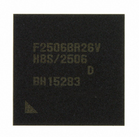
DF2506BR26DV Renesas Electronics America, DF2506BR26DV Datasheet - Page 502

DF2506BR26DV
Manufacturer Part Number
DF2506BR26DV
Description
IC H8S/2506 MCU FLASH 176-LFBGA
Manufacturer
Renesas Electronics America
Series
H8® H8S/2500r
Specifications of DF2506BR26DV
Core Processor
H8S/2000
Core Size
16-Bit
Speed
26MHz
Connectivity
I²C, SCI
Peripherals
POR, PWM, WDT
Number Of I /o
104
Program Memory Size
512KB (512K x 8)
Program Memory Type
FLASH
Ram Size
32K x 8
Voltage - Supply (vcc/vdd)
3 V ~ 5.5 V
Data Converters
A/D 16x10b; D/A 2x8b
Oscillator Type
Internal
Operating Temperature
-40°C ~ 85°C
Package / Case
176-LFBGA
Lead Free Status / RoHS Status
Lead free / RoHS Compliant
Eeprom Size
-
Available stocks
Company
Part Number
Manufacturer
Quantity
Price
Company:
Part Number:
DF2506BR26DV
Manufacturer:
Renesas Electronics America
Quantity:
10 000
- Current page: 502 of 980
- Download datasheet (6Mb)
Section 13 Serial Communication Interface (SCI)
13.7.2
Figure 13.22 shows the transfer data format in Smart Card interface mode.
• One frame consists of 8-bit data plus a parity bit in asynchronous mode.
• In transmission, a guard time of at least 2 etu (Elementary time unit: the time for transfer of
• If a parity error is detected during reception, a low error signal level is output for one etu
• If an error signal is sampled during transmission, the same data is retransmitted automatically
Rev. 6.00 Sep. 24, 2009 Page 454 of 928
REJ09B0099-0600
one bit) is left between the end of the parity bit and the start of the next frame.
period, 10.5 etu after the start bit.
after a delay of 2 etu or longer.
Figure 13.21 (2) Schematic Diagram of Smart Card Interface Pin Connections
Data Format (Except for Block Transfer Mode)
When there is no parity error
When a parity error occurs
Legend:
DS
D0 to D7
Dp
DE
Figure 13.22 Normal Smart Card Interface Data Format
: Start bit
: Data bits
: Parity bit
: Error signal
Ds
Ds
Connected equipment
This LSI
D0
D0
D1
D1
Px (port)
Transmitting station output
Transmitting station output
SCK
RxD
TxD
D2
D2
D3
D3
(Channel 2)
D4
D4
Data line
Clock line
Reset line
P1 V
D5
D5
CC
D6
D6
D7
D7
I/O
CLK
RST
Dp
Dp
IC card
Receiving station
output
DE
Related parts for DF2506BR26DV
Image
Part Number
Description
Manufacturer
Datasheet
Request
R

Part Number:
Description:
KIT STARTER FOR M16C/29
Manufacturer:
Renesas Electronics America
Datasheet:

Part Number:
Description:
KIT STARTER FOR R8C/2D
Manufacturer:
Renesas Electronics America
Datasheet:

Part Number:
Description:
R0K33062P STARTER KIT
Manufacturer:
Renesas Electronics America
Datasheet:

Part Number:
Description:
KIT STARTER FOR R8C/23 E8A
Manufacturer:
Renesas Electronics America
Datasheet:

Part Number:
Description:
KIT STARTER FOR R8C/25
Manufacturer:
Renesas Electronics America
Datasheet:

Part Number:
Description:
KIT STARTER H8S2456 SHARPE DSPLY
Manufacturer:
Renesas Electronics America
Datasheet:

Part Number:
Description:
KIT STARTER FOR R8C38C
Manufacturer:
Renesas Electronics America
Datasheet:

Part Number:
Description:
KIT STARTER FOR R8C35C
Manufacturer:
Renesas Electronics America
Datasheet:

Part Number:
Description:
KIT STARTER FOR R8CL3AC+LCD APPS
Manufacturer:
Renesas Electronics America
Datasheet:

Part Number:
Description:
KIT STARTER FOR RX610
Manufacturer:
Renesas Electronics America
Datasheet:

Part Number:
Description:
KIT STARTER FOR R32C/118
Manufacturer:
Renesas Electronics America
Datasheet:

Part Number:
Description:
KIT DEV RSK-R8C/26-29
Manufacturer:
Renesas Electronics America
Datasheet:

Part Number:
Description:
KIT STARTER FOR SH7124
Manufacturer:
Renesas Electronics America
Datasheet:

Part Number:
Description:
KIT STARTER FOR H8SX/1622
Manufacturer:
Renesas Electronics America
Datasheet:

Part Number:
Description:
KIT DEV FOR SH7203
Manufacturer:
Renesas Electronics America
Datasheet:


