DF2506BR26DV Renesas Electronics America, DF2506BR26DV Datasheet - Page 451
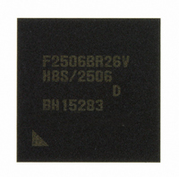
DF2506BR26DV
Manufacturer Part Number
DF2506BR26DV
Description
IC H8S/2506 MCU FLASH 176-LFBGA
Manufacturer
Renesas Electronics America
Series
H8® H8S/2500r
Specifications of DF2506BR26DV
Core Processor
H8S/2000
Core Size
16-Bit
Speed
26MHz
Connectivity
I²C, SCI
Peripherals
POR, PWM, WDT
Number Of I /o
104
Program Memory Size
512KB (512K x 8)
Program Memory Type
FLASH
Ram Size
32K x 8
Voltage - Supply (vcc/vdd)
3 V ~ 5.5 V
Data Converters
A/D 16x10b; D/A 2x8b
Oscillator Type
Internal
Operating Temperature
-40°C ~ 85°C
Package / Case
176-LFBGA
Lead Free Status / RoHS Status
Lead free / RoHS Compliant
Eeprom Size
-
Available stocks
Company
Part Number
Manufacturer
Quantity
Price
Company:

Part Number:
DF2506BR26DV
Manufacturer:
Renesas Electronics America
Quantity:
10 000


• Smart Card Interface Mode (When SMIF in SCMR Is 1)
Bit
7
6
Bit Name
GM
BLK
Initial
Value
0
0
R/W
R/W
R/W
0: Normal smart card interface mode operation (initial
0: Normal smart card interface mode operation (initial
Description
GS Mode
Setting this bit to 1 allows GSM mode operation. In GSM
mode, the TEND set timing is put forward to 11.0 etu
from the start and the clock output control function is
appended. For details, see section 13.7.8, Clock Output
Control.
•
•
1: GSM mode operation in smart card interface mode
•
•
Setting this bit to 1 allows block transfer mode operation.
For details, see section 13.7.3, Block Transfer Mode.
•
•
•
1: Operation in block transfer mode
•
•
•
value)
value)
The TEND flag is generated 12.5 etu (11.5 etu in the
block transfer mode) after the beginning of the start
bit.
Clock output on/off control only
The TEND flag is generated 11.0 etu after the
beginning of the start bit.
In addition to clock output on/off control, high/low
fixed control is supported (set using SCR).
Error signal transmission, detection, and automatic
data retransmission are performed.
The TXI interrupt is generated by the TEND flag.
The TEND flag is set 12.5 etu (11.0 etu in the GSM
mode) after transmission starts.
Error signal transmission, detection, and automatic
data retransmission are not performed.
The TXI interrupt is generated by the TDRE flag.
The TEND flag is set 11.5 etu (11.0 etu in the GSM
mode) after transmission starts.
Section 13 Serial Communication Interface (SCI)
Rev. 6.00 Sep. 24, 2009 Page 403 of 928
REJ09B0099-0600
Related parts for DF2506BR26DV
Image
Part Number
Description
Manufacturer
Datasheet
Request
R

Part Number:
Description:
KIT STARTER FOR M16C/29
Manufacturer:
Renesas Electronics America
Datasheet:

Part Number:
Description:
KIT STARTER FOR R8C/2D
Manufacturer:
Renesas Electronics America
Datasheet:

Part Number:
Description:
R0K33062P STARTER KIT
Manufacturer:
Renesas Electronics America
Datasheet:

Part Number:
Description:
KIT STARTER FOR R8C/23 E8A
Manufacturer:
Renesas Electronics America
Datasheet:

Part Number:
Description:
KIT STARTER FOR R8C/25
Manufacturer:
Renesas Electronics America
Datasheet:

Part Number:
Description:
KIT STARTER H8S2456 SHARPE DSPLY
Manufacturer:
Renesas Electronics America
Datasheet:

Part Number:
Description:
KIT STARTER FOR R8C38C
Manufacturer:
Renesas Electronics America
Datasheet:

Part Number:
Description:
KIT STARTER FOR R8C35C
Manufacturer:
Renesas Electronics America
Datasheet:

Part Number:
Description:
KIT STARTER FOR R8CL3AC+LCD APPS
Manufacturer:
Renesas Electronics America
Datasheet:
Part Number:
Description:
KIT STARTER FOR RX610
Manufacturer:
Renesas Electronics America
Datasheet:

Part Number:
Description:
KIT STARTER FOR R32C/118
Manufacturer:
Renesas Electronics America
Datasheet:

Part Number:
Description:
KIT DEV RSK-R8C/26-29
Manufacturer:
Renesas Electronics America
Datasheet:

Part Number:
Description:
KIT STARTER FOR SH7124
Manufacturer:
Renesas Electronics America
Datasheet:

Part Number:
Description:
KIT STARTER FOR H8SX/1622
Manufacturer:
Renesas Electronics America
Datasheet:

Part Number:
Description:
KIT DEV FOR SH7203
Manufacturer:
Renesas Electronics America
Datasheet: