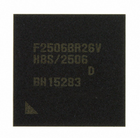
DF2506BR26DV Renesas Electronics America, DF2506BR26DV Datasheet - Page 353

DF2506BR26DV
Manufacturer Part Number
DF2506BR26DV
Description
IC H8S/2506 MCU FLASH 176-LFBGA
Manufacturer
Renesas Electronics America
Series
H8® H8S/2500r
Specifications of DF2506BR26DV
Core Processor
H8S/2000
Core Size
16-Bit
Speed
26MHz
Connectivity
I²C, SCI
Peripherals
POR, PWM, WDT
Number Of I /o
104
Program Memory Size
512KB (512K x 8)
Program Memory Type
FLASH
Ram Size
32K x 8
Voltage - Supply (vcc/vdd)
3 V ~ 5.5 V
Data Converters
A/D 16x10b; D/A 2x8b
Oscillator Type
Internal
Operating Temperature
-40°C ~ 85°C
Package / Case
176-LFBGA
Lead Free Status / RoHS Status
Lead free / RoHS Compliant
Eeprom Size
-
Available stocks
Company
Part Number
Manufacturer
Quantity
Price
Company:
Part Number:
DF2506BR26DV
Manufacturer:
Renesas Electronics America
Quantity:
10 000
- Current page: 353 of 980
- Download datasheet (6Mb)
10.3.6
The TCNT registers are 16-bit readable/writable counters. The TPU has six TCNT counters, one
for each channel.
The TCNT counters are initialized to H'0000 by a reset, and in hardware standby mode.
The TCNT counters cannot be accessed in 8-bit units; they must always be accessed as a 16-bit
unit.
10.3.7
The TGR registers are dual function 16-bit readable/writable registers, functioning as either output
compare or input capture registers. The TPU has 16 TGR registers, four each for channels 0 and 3
and two each for channels 1, 2, 4, and 5. TGRC and TGRD for channels 0 and 3 can also be
designated for operation as buffer registers. The TGR registers cannot be accessed in 8-bit units;
they must always be accessed as a 16-bit unit. TGR buffer register combinations are TGRA—
TGRC and TGRB—TGRD.
10.3.8
TSTR specifies whether to operate or stop TCNT for channels 0 to 5. When setting the operating
mode in TMDR or setting the count clock in TCR, first stop the TCNT counter.
Bit
7, 6
5
4
3
2
1
0
Bit Name
⎯
CST5
CST4
CST3
CST2
CST1
CST0
Timer Counter (TCNT)
Timer General Register (TGR)
Timer Start Register (TSTR)
Initial
value
All 0
0
0
0
0
0
0
R/W
⎯
R/W
R/W
R/W
R/W
R/W
R/W
Description
Reserved
Only 0 should be written to these bits.
Counter Start 5 to 0
These bits specify whether to operate or stop TCNT.
If 0 is written to the CST bit during operation with the TIOC
pin designated for output, the counter stops but the TIOC
pin output compare output level is retained. If TIOR is
written to when the CST bit is cleared to 0, the pin output
level will be changed to the set initial output value.
0: TCNT_0 to TCNT_5 count operation is stopped
1: TCNT_0 to TCNT_5 performs count operation
Rev. 6.00 Sep. 24, 2009 Page 305 of 928
Section 10 16-Bit Timer Pulse Unit (TPU)
REJ09B0099-0600
Related parts for DF2506BR26DV
Image
Part Number
Description
Manufacturer
Datasheet
Request
R

Part Number:
Description:
KIT STARTER FOR M16C/29
Manufacturer:
Renesas Electronics America
Datasheet:

Part Number:
Description:
KIT STARTER FOR R8C/2D
Manufacturer:
Renesas Electronics America
Datasheet:

Part Number:
Description:
R0K33062P STARTER KIT
Manufacturer:
Renesas Electronics America
Datasheet:

Part Number:
Description:
KIT STARTER FOR R8C/23 E8A
Manufacturer:
Renesas Electronics America
Datasheet:

Part Number:
Description:
KIT STARTER FOR R8C/25
Manufacturer:
Renesas Electronics America
Datasheet:

Part Number:
Description:
KIT STARTER H8S2456 SHARPE DSPLY
Manufacturer:
Renesas Electronics America
Datasheet:

Part Number:
Description:
KIT STARTER FOR R8C38C
Manufacturer:
Renesas Electronics America
Datasheet:

Part Number:
Description:
KIT STARTER FOR R8C35C
Manufacturer:
Renesas Electronics America
Datasheet:

Part Number:
Description:
KIT STARTER FOR R8CL3AC+LCD APPS
Manufacturer:
Renesas Electronics America
Datasheet:

Part Number:
Description:
KIT STARTER FOR RX610
Manufacturer:
Renesas Electronics America
Datasheet:

Part Number:
Description:
KIT STARTER FOR R32C/118
Manufacturer:
Renesas Electronics America
Datasheet:

Part Number:
Description:
KIT DEV RSK-R8C/26-29
Manufacturer:
Renesas Electronics America
Datasheet:

Part Number:
Description:
KIT STARTER FOR SH7124
Manufacturer:
Renesas Electronics America
Datasheet:

Part Number:
Description:
KIT STARTER FOR H8SX/1622
Manufacturer:
Renesas Electronics America
Datasheet:

Part Number:
Description:
KIT DEV FOR SH7203
Manufacturer:
Renesas Electronics America
Datasheet:


