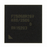
DF2506BR26DV Renesas Electronics America, DF2506BR26DV Datasheet - Page 923

DF2506BR26DV
Manufacturer Part Number
DF2506BR26DV
Description
IC H8S/2506 MCU FLASH 176-LFBGA
Manufacturer
Renesas Electronics America
Series
H8® H8S/2500r
Specifications of DF2506BR26DV
Core Processor
H8S/2000
Core Size
16-Bit
Speed
26MHz
Connectivity
I²C, SCI
Peripherals
POR, PWM, WDT
Number Of I /o
104
Program Memory Size
512KB (512K x 8)
Program Memory Type
FLASH
Ram Size
32K x 8
Voltage - Supply (vcc/vdd)
3 V ~ 5.5 V
Data Converters
A/D 16x10b; D/A 2x8b
Oscillator Type
Internal
Operating Temperature
-40°C ~ 85°C
Package / Case
176-LFBGA
Lead Free Status / RoHS Status
Lead free / RoHS Compliant
Eeprom Size
-
Available stocks
Company
Part Number
Manufacturer
Quantity
Price
Company:
Part Number:
DF2506BR26DV
Manufacturer:
Renesas Electronics America
Quantity:
10 000
- Current page: 923 of 980
- Download datasheet (6Mb)
Notes: 1. The regular specifications are supported in the H8S/2506 Group only.
Item
Output high
voltage*
Output low
voltage*
Input leakage
current
Three-state
leakage
current
(off state)
Input pull-up
MOS current
6
6
2. If the A/D and D/A converters are not used, do not leave the AV
3. P35/SCK1/SCL0 and P34/SDA0 are NMOS push/pull outputs.
4. When ICE = 0. To output low when bus drive function is selected is determined in table
5. HRxD and HTxD are supported in the H8S/2556 Group only.
6. When P1V
open. Apply a voltage 3.0 V to 5.5 V to the AV
for instance. Set V
To output high level signal, pull-up resistance must be connected externally.
24.4, Bus Drive Characteristics.
in ICPCR is 1), P2V
V (BUFGC2 in ICPCR is 1).
Ports 1 to 3, 7
Ports 5, A to H, J,
HTxD*
P34, P35*
All output
pins*
RES
STBY, NMI,
MD2 to MD0,
TEST
HRxD*
Ports 4, 9
Ports 1 to 3, 7
Ports 5, A to H, J
Ports A to E
4
5
5
CC
= 5.0 V ±0.5 V (BUFGC1 in ICPCR is 0), P1V
3
ref
CC
≤ AV
Symbol Min.
V
V
| l
| l
–l
= 5.0 V ±0.5 V (BUFGC2 in ICPCR is 0), and P2V
OH
OL
in
TSI
P
|
CC
|
.
P2V
P2V
P1V
P1V
P2V
P2V
⎯
⎯
⎯
⎯
⎯
⎯
⎯
10
CC
CC
CC
CC
CC
CC
- 0.5
- 1.0
- 0.5
- 1.0
- 2.7
- 2.0
Typ.
⎯
⎯
⎯
⎯
⎯
⎯
⎯
⎯
⎯
⎯
⎯
⎯
⎯
⎯
CC
and V
Rev. 6.00 Sep. 24, 2009 Page 875 of 928
Max.
⎯
⎯
⎯
⎯
⎯
⎯
0.4
1.0
1.0
1.0
1.0
1.0
1.0
300
ref
Section 24 Electrical Characteristics
pins by connecting them to V
CC
= 3.3 V ±0.3 V (BUFGC1
CC
Unit
V
V
V
V
V
V
V
μA
μA
μA
μA
μA
μA
μA
, V
ref
, and AV
Test Conditions
I
I
I
I
I
P2V
I
P2V
I
V
V
V
V
V
- 0.2 V
V
- 0.2 V
V
- 0.2 V
V
- 0.2 V
V
OH
OH
OH
OH
OH
OH
OL
REJ09B0099-0600
in
in
in
in
in
in
in
CC
= - 200 μA
= - 1 mA
= - 200 μA
= - 1 mA
= - 100 μA
= - 100 μA
= 0.8 mA
= 0.2 to V
= 0.2 to V
= 0.2 to P1V
= 0.2 to AV
= 0.2 to P2V
= 0.2 to P1V
= 0 V
CC
CC
= 3.3 V ±0.3
= 5.0 V ± 0.5 V
= 3.3 V ± 0.3 V
SS
pins
CC
CC
CC
- 0.2
- 0.2
CC
CC
CC
CC
,
Related parts for DF2506BR26DV
Image
Part Number
Description
Manufacturer
Datasheet
Request
R

Part Number:
Description:
KIT STARTER FOR M16C/29
Manufacturer:
Renesas Electronics America
Datasheet:

Part Number:
Description:
KIT STARTER FOR R8C/2D
Manufacturer:
Renesas Electronics America
Datasheet:

Part Number:
Description:
R0K33062P STARTER KIT
Manufacturer:
Renesas Electronics America
Datasheet:

Part Number:
Description:
KIT STARTER FOR R8C/23 E8A
Manufacturer:
Renesas Electronics America
Datasheet:

Part Number:
Description:
KIT STARTER FOR R8C/25
Manufacturer:
Renesas Electronics America
Datasheet:

Part Number:
Description:
KIT STARTER H8S2456 SHARPE DSPLY
Manufacturer:
Renesas Electronics America
Datasheet:

Part Number:
Description:
KIT STARTER FOR R8C38C
Manufacturer:
Renesas Electronics America
Datasheet:

Part Number:
Description:
KIT STARTER FOR R8C35C
Manufacturer:
Renesas Electronics America
Datasheet:

Part Number:
Description:
KIT STARTER FOR R8CL3AC+LCD APPS
Manufacturer:
Renesas Electronics America
Datasheet:

Part Number:
Description:
KIT STARTER FOR RX610
Manufacturer:
Renesas Electronics America
Datasheet:

Part Number:
Description:
KIT STARTER FOR R32C/118
Manufacturer:
Renesas Electronics America
Datasheet:

Part Number:
Description:
KIT DEV RSK-R8C/26-29
Manufacturer:
Renesas Electronics America
Datasheet:

Part Number:
Description:
KIT STARTER FOR SH7124
Manufacturer:
Renesas Electronics America
Datasheet:

Part Number:
Description:
KIT STARTER FOR H8SX/1622
Manufacturer:
Renesas Electronics America
Datasheet:

Part Number:
Description:
KIT DEV FOR SH7203
Manufacturer:
Renesas Electronics America
Datasheet:


