DF2506BR26DV Renesas Electronics America, DF2506BR26DV Datasheet - Page 76
DF2506BR26DV
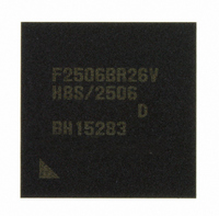
Manufacturer Part Number
DF2506BR26DV
Description
IC H8S/2506 MCU FLASH 176-LFBGA
Manufacturer
Renesas Electronics America
Series
H8® H8S/2500r
Specifications of DF2506BR26DV
Core Processor
H8S/2000
Core Size
16-Bit
Speed
26MHz
Connectivity
I²C, SCI
Peripherals
POR, PWM, WDT
Number Of I /o
104
Program Memory Size
512KB (512K x 8)
Program Memory Type
FLASH
Ram Size
32K x 8
Voltage - Supply (vcc/vdd)
3 V ~ 5.5 V
Data Converters
A/D 16x10b; D/A 2x8b
Oscillator Type
Internal
Operating Temperature
-40°C ~ 85°C
Package / Case
176-LFBGA
Lead Free Status / RoHS Status
Lead free / RoHS Compliant
Eeprom Size
-
Available stocks
Company
Part Number
Manufacturer
Quantity
Price
Company:

Part Number:
DF2506BR26DV
Manufacturer:
Renesas Electronics America
Quantity:
10 000


Section 2 CPU
2.2
The H8S/2000 CPU has two operating modes: normal and advanced. Normal mode supports a
maximum 64-kbyte address space. Advanced mode supports a maximum 16-Mbyte total address
space. The mode is selected by the mode pins.
2.2.1
The exception vector table and stack have the same structure as in the H8/300 CPU.
• Address Space
• Extended Registers (En)
• Instruction Set
• Exception Vector Table and Memory Indirect Branch Addresses
• Stack Structure
Rev. 6.00 Sep. 24, 2009 Page 28 of 928
REJ09B0099-0600
Linear access is provided to a maximum address space of 64 kbytes.
The extended registers (E0 to E7) can be used as 16-bit registers, or as the upper 16-bit
segments of 32-bit registers. When En is used as a 16-bit register it can contain any value, even
when the corresponding general register (Rn) is used as an address register. If the general
register is referenced in the register indirect addressing mode with pre-decrement (@–Rn) or
post-increment (@Rn+) and a carry or borrow occurs, however, the value in the corresponding
extended register (En) will be affected.
All instructions and addressing modes can be used. Only the lower 16 bits of effective
addresses (EA) are valid.
In normal mode the top area starting at H'0000 is allocated to the exception vector table. One
branch address is stored per 16 bits. Figure 2.1 shows the structure of the exception vector
table in normal mode. For details of the exception vector table, see section 4, Exception
Handling.
The memory indirect addressing mode (@@aa:8) employed in the JMP and JSR instructions
uses an 8-bit absolute address included in the instruction code to specify a memory operand
that contains a branch address. In normal mode the operand is a 16-bit word operand,
providing a 16-bit branch address. Branch addresses can be stored in the top area from H'0000
to H'00FF. Note that this area is also used for the exception vector table.
When the program counter (PC) is pushed onto the stack in a subroutine call, and the PC,
condition-code register (CCR) and extended control register (EXR) are pushed onto the stack
in exception handling, they are stored as shown in figure 2.2. EXR is not pushed onto the stack
in interrupt control mode 0. For details, see section 4, Exception Handling.
CPU Operating Modes
Normal Mode
Related parts for DF2506BR26DV
Image
Part Number
Description
Manufacturer
Datasheet
Request
R

Part Number:
Description:
KIT STARTER FOR M16C/29
Manufacturer:
Renesas Electronics America
Datasheet:

Part Number:
Description:
KIT STARTER FOR R8C/2D
Manufacturer:
Renesas Electronics America
Datasheet:

Part Number:
Description:
R0K33062P STARTER KIT
Manufacturer:
Renesas Electronics America
Datasheet:

Part Number:
Description:
KIT STARTER FOR R8C/23 E8A
Manufacturer:
Renesas Electronics America
Datasheet:

Part Number:
Description:
KIT STARTER FOR R8C/25
Manufacturer:
Renesas Electronics America
Datasheet:

Part Number:
Description:
KIT STARTER H8S2456 SHARPE DSPLY
Manufacturer:
Renesas Electronics America
Datasheet:

Part Number:
Description:
KIT STARTER FOR R8C38C
Manufacturer:
Renesas Electronics America
Datasheet:

Part Number:
Description:
KIT STARTER FOR R8C35C
Manufacturer:
Renesas Electronics America
Datasheet:

Part Number:
Description:
KIT STARTER FOR R8CL3AC+LCD APPS
Manufacturer:
Renesas Electronics America
Datasheet:
Part Number:
Description:
KIT STARTER FOR RX610
Manufacturer:
Renesas Electronics America
Datasheet:

Part Number:
Description:
KIT STARTER FOR R32C/118
Manufacturer:
Renesas Electronics America
Datasheet:

Part Number:
Description:
KIT DEV RSK-R8C/26-29
Manufacturer:
Renesas Electronics America
Datasheet:

Part Number:
Description:
KIT STARTER FOR SH7124
Manufacturer:
Renesas Electronics America
Datasheet:

Part Number:
Description:
KIT STARTER FOR H8SX/1622
Manufacturer:
Renesas Electronics America
Datasheet:

Part Number:
Description:
KIT DEV FOR SH7203
Manufacturer:
Renesas Electronics America
Datasheet: