DF2506BR26DV Renesas Electronics America, DF2506BR26DV Datasheet - Page 20
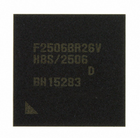
DF2506BR26DV
Manufacturer Part Number
DF2506BR26DV
Description
IC H8S/2506 MCU FLASH 176-LFBGA
Manufacturer
Renesas Electronics America
Series
H8® H8S/2500r
Specifications of DF2506BR26DV
Core Processor
H8S/2000
Core Size
16-Bit
Speed
26MHz
Connectivity
I²C, SCI
Peripherals
POR, PWM, WDT
Number Of I /o
104
Program Memory Size
512KB (512K x 8)
Program Memory Type
FLASH
Ram Size
32K x 8
Voltage - Supply (vcc/vdd)
3 V ~ 5.5 V
Data Converters
A/D 16x10b; D/A 2x8b
Oscillator Type
Internal
Operating Temperature
-40°C ~ 85°C
Package / Case
176-LFBGA
Lead Free Status / RoHS Status
Lead free / RoHS Compliant
Eeprom Size
-
Available stocks
Company
Part Number
Manufacturer
Quantity
Price
Company:

Part Number:
DF2506BR26DV
Manufacturer:
Renesas Electronics America
Quantity:
10 000


Section 12 Watchdog Timer (WDT) ................................................................... 377
12.1 Features.............................................................................................................................. 377
12.2 Input/Output Pin ................................................................................................................ 379
12.3 Register Descriptions......................................................................................................... 380
12.4 Operation ........................................................................................................................... 386
12.5 Interrupt Sources................................................................................................................ 389
12.6 Usage Notes ....................................................................................................................... 390
Section 13 Serial Communication Interface (SCI).............................................. 395
13.1 Features.............................................................................................................................. 395
13.2 Input/Output Pins............................................................................................................... 397
13.3 Register Descriptions......................................................................................................... 398
13.4 Operation in Asynchronous Mode ..................................................................................... 425
Rev. 6.00 Sep. 24, 2009 Page xviii of xlvi
REJ09B0099-0600
11.8.6 Switching of Internal Clocks and TCNT Operation ............................................. 374
11.8.7 Contention between Interrupts and Module Stop Mode ....................................... 376
11.8.8 Mode Setting in Cascading ................................................................................... 376
12.3.1 Timer Counter (TCNT)......................................................................................... 380
12.3.2 Timer Control/Status Register .............................................................................. 380
12.3.3 Reset Control/Status Register (RSTCSR) (WDT_0 only) .................................... 385
12.4.1 Watchdog Timer Mode......................................................................................... 386
12.4.2 Interval Timer Mode............................................................................................. 387
12.4.3 Timing of Setting Overflow Flag (OVF) .............................................................. 388
12.4.4 Timing of Setting Watchdog Timer Overflow Flag (WOVF) .............................. 389
12.6.1 Notes on Register Access ..................................................................................... 390
12.6.2 Contention between Timer Counter (TCNT) Write and Increment ...................... 392
12.6.3 Changing Value of PSS or CKS2 to CKS0........................................................... 392
12.6.4 Switching between Watchdog Timer Mode and Interval Timer Mode................. 392
12.6.5 Internal Reset in Watchdog Timer Mode.............................................................. 393
12.6.6 OVF Flag Clearing in Interval Timer Mode ......................................................... 393
12.6.7 Initialization of TCNT by the TME Bit ................................................................ 393
13.3.1 Receive Shift Register (RSR) ............................................................................... 399
13.3.2 Receive Data Register (RDR)............................................................................... 399
13.3.3 Transmit Data Register (TDR).............................................................................. 400
13.3.4 Transmit Shift Register (TSR) .............................................................................. 400
13.3.5 Serial Mode Register (SMR) ................................................................................ 400
13.3.6 Serial Control Register (SCR) .............................................................................. 405
13.3.7 Serial Status Register (SSR) ................................................................................. 410
13.3.8 Smart Card Mode Register (SCMR)..................................................................... 417
13.3.9 Bit Rate Register (BRR) ....................................................................................... 418
Related parts for DF2506BR26DV
Image
Part Number
Description
Manufacturer
Datasheet
Request
R

Part Number:
Description:
KIT STARTER FOR M16C/29
Manufacturer:
Renesas Electronics America
Datasheet:

Part Number:
Description:
KIT STARTER FOR R8C/2D
Manufacturer:
Renesas Electronics America
Datasheet:

Part Number:
Description:
R0K33062P STARTER KIT
Manufacturer:
Renesas Electronics America
Datasheet:

Part Number:
Description:
KIT STARTER FOR R8C/23 E8A
Manufacturer:
Renesas Electronics America
Datasheet:

Part Number:
Description:
KIT STARTER FOR R8C/25
Manufacturer:
Renesas Electronics America
Datasheet:

Part Number:
Description:
KIT STARTER H8S2456 SHARPE DSPLY
Manufacturer:
Renesas Electronics America
Datasheet:

Part Number:
Description:
KIT STARTER FOR R8C38C
Manufacturer:
Renesas Electronics America
Datasheet:

Part Number:
Description:
KIT STARTER FOR R8C35C
Manufacturer:
Renesas Electronics America
Datasheet:

Part Number:
Description:
KIT STARTER FOR R8CL3AC+LCD APPS
Manufacturer:
Renesas Electronics America
Datasheet:
Part Number:
Description:
KIT STARTER FOR RX610
Manufacturer:
Renesas Electronics America
Datasheet:

Part Number:
Description:
KIT STARTER FOR R32C/118
Manufacturer:
Renesas Electronics America
Datasheet:

Part Number:
Description:
KIT DEV RSK-R8C/26-29
Manufacturer:
Renesas Electronics America
Datasheet:

Part Number:
Description:
KIT STARTER FOR SH7124
Manufacturer:
Renesas Electronics America
Datasheet:

Part Number:
Description:
KIT STARTER FOR H8SX/1622
Manufacturer:
Renesas Electronics America
Datasheet:

Part Number:
Description:
KIT DEV FOR SH7203
Manufacturer:
Renesas Electronics America
Datasheet: