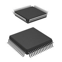
HD64F3644H Renesas Electronics America, HD64F3644H Datasheet - Page 142

HD64F3644H
Manufacturer Part Number
HD64F3644H
Description
IC H8 MCU FLASH 32K 64-QFP
Manufacturer
Renesas Electronics America
Series
H8® H8/300Lr
Datasheet
1.HD64F3644HV.pdf
(551 pages)
Specifications of HD64F3644H
Core Processor
H8/300L
Core Size
8-Bit
Speed
8MHz
Connectivity
SCI
Peripherals
PWM, WDT
Number Of I /o
53
Program Memory Size
32KB (32K x 8)
Program Memory Type
FLASH
Ram Size
1K x 8
Voltage - Supply (vcc/vdd)
2.7 V ~ 5.5 V
Data Converters
A/D 8x8b
Oscillator Type
Internal
Operating Temperature
-20°C ~ 75°C
Package / Case
64-QFP
Package
64PQFP
Family Name
H8
Maximum Speed
8 MHz
Operating Supply Voltage
3.3|5 V
Data Bus Width
8 Bit
Number Of Programmable I/os
45
Interface Type
SCI
On-chip Adc
8-chx8-bit
Number Of Timers
4
Lead Free Status / RoHS Status
Contains lead / RoHS non-compliant
Eeprom Size
-
Available stocks
Company
Part Number
Manufacturer
Quantity
Price
Company:
Part Number:
HD64F3644H
Manufacturer:
HITACHI
Quantity:
490
Company:
Part Number:
HD64F3644H
Manufacturer:
Renesas Electronics America
Quantity:
10 000
Part Number:
HD64F3644H
Manufacturer:
HD
Quantity:
20 000
Company:
Part Number:
HD64F3644HV
Manufacturer:
Renesas
Quantity:
600
Company:
Part Number:
HD64F3644HV
Manufacturer:
Renesas Electronics America
Quantity:
10 000
Part Number:
HD64F3644HV
Manufacturer:
RENESAS/瑞萨
Quantity:
20 000
Part Number:
HD64F3644HV/H83644
Manufacturer:
RENESAS/瑞萨
Quantity:
20 000
- Current page: 142 of 551
- Download datasheet (4Mb)
Section 6 ROM
6.6
When an on-board programming mode is selected, on-chip flash memory programming, erasing,
and verifying can be carried out. There are two on-board programming modes boot mode and
user program mode set by the mode pin (TEST) and the FV
the on-board programming modes. For information on turning V
6.9, Flash Memory Programming and Erasing Precautions.
Table 6.9
Mode Setting
Boot mode
User program mode
Note:
6.6.1
When boot mode is used, a user program for flash memory programming and erasing must be
prepared beforehand in the host machine (which may be a personal computer). SCI3 is used in
asynchronous mode (see figure 6.8). When the H8/3644F, H8/3643F, or H8/3642AF is set to boot
mode, after reset release a built-in boot program is activated, the low period of the data sent from
the host is first measured, and the bit rate register (BRR) value determined. The chip’s on-chip
serial communication interface (SCI3) can then be used to download the user program from the
host machine. The downloaded user program is written into RAM.
After the program has been stored, execution branches to the start address (H'FBE0) of the on-chip
RAM, the program stored in RAM is executed, and flash memory programming/erasing can be
carried out. Figure 6.9 shows the boot mode execution procedure.
Rev. 6.00 Sep 12, 2006 page 120 of 526
REJ09B0326-0600
* See notes 6 to 8 in section 6.6.1, Notes on Use of Boot Mode, for the timing of 12 V
On-Board Programming Modes
Boot Mode
application.
HOST
On-Board Programming Mode Selection
Figure 6.8 Boot Mode System Configuration
Reception of programming data
FV
12 V *
Transmission of verify data
PP
TEST
12 V *
V
SS
PP
pin. Table 6.9 shows how to select
PP
on and off, see note 5 in section
RXD
TXD
H8/3643F, or
H8/3642AF
H8/3644F,
Notes
SCI3
Related parts for HD64F3644H
Image
Part Number
Description
Manufacturer
Datasheet
Request
R

Part Number:
Description:
(HD64 Series) Hitachi Single-Chip Microcomputer
Manufacturer:
Hitachi Semiconductor
Datasheet:

Part Number:
Description:
KIT STARTER FOR M16C/29
Manufacturer:
Renesas Electronics America
Datasheet:

Part Number:
Description:
KIT STARTER FOR R8C/2D
Manufacturer:
Renesas Electronics America
Datasheet:

Part Number:
Description:
R0K33062P STARTER KIT
Manufacturer:
Renesas Electronics America
Datasheet:

Part Number:
Description:
KIT STARTER FOR R8C/23 E8A
Manufacturer:
Renesas Electronics America
Datasheet:

Part Number:
Description:
KIT STARTER FOR R8C/25
Manufacturer:
Renesas Electronics America
Datasheet:

Part Number:
Description:
KIT STARTER H8S2456 SHARPE DSPLY
Manufacturer:
Renesas Electronics America
Datasheet:

Part Number:
Description:
KIT STARTER FOR R8C38C
Manufacturer:
Renesas Electronics America
Datasheet:

Part Number:
Description:
KIT STARTER FOR R8C35C
Manufacturer:
Renesas Electronics America
Datasheet:

Part Number:
Description:
KIT STARTER FOR R8CL3AC+LCD APPS
Manufacturer:
Renesas Electronics America
Datasheet:

Part Number:
Description:
KIT STARTER FOR RX610
Manufacturer:
Renesas Electronics America
Datasheet:

Part Number:
Description:
KIT STARTER FOR R32C/118
Manufacturer:
Renesas Electronics America
Datasheet:

Part Number:
Description:
KIT DEV RSK-R8C/26-29
Manufacturer:
Renesas Electronics America
Datasheet:

Part Number:
Description:
KIT STARTER FOR SH7124
Manufacturer:
Renesas Electronics America
Datasheet:

Part Number:
Description:
KIT STARTER FOR H8SX/1622
Manufacturer:
Renesas Electronics America
Datasheet:


