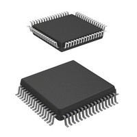
HD64F3644H Renesas Electronics America, HD64F3644H Datasheet - Page 35

HD64F3644H
Manufacturer Part Number
HD64F3644H
Description
IC H8 MCU FLASH 32K 64-QFP
Manufacturer
Renesas Electronics America
Series
H8® H8/300Lr
Datasheet
1.HD64F3644HV.pdf
(551 pages)
Specifications of HD64F3644H
Core Processor
H8/300L
Core Size
8-Bit
Speed
8MHz
Connectivity
SCI
Peripherals
PWM, WDT
Number Of I /o
53
Program Memory Size
32KB (32K x 8)
Program Memory Type
FLASH
Ram Size
1K x 8
Voltage - Supply (vcc/vdd)
2.7 V ~ 5.5 V
Data Converters
A/D 8x8b
Oscillator Type
Internal
Operating Temperature
-20°C ~ 75°C
Package / Case
64-QFP
Package
64PQFP
Family Name
H8
Maximum Speed
8 MHz
Operating Supply Voltage
3.3|5 V
Data Bus Width
8 Bit
Number Of Programmable I/os
45
Interface Type
SCI
On-chip Adc
8-chx8-bit
Number Of Timers
4
Lead Free Status / RoHS Status
Contains lead / RoHS non-compliant
Eeprom Size
-
Available stocks
Company
Part Number
Manufacturer
Quantity
Price
Company:
Part Number:
HD64F3644H
Manufacturer:
HITACHI
Quantity:
490
Company:
Part Number:
HD64F3644H
Manufacturer:
Renesas Electronics America
Quantity:
10 000
Part Number:
HD64F3644H
Manufacturer:
HD
Quantity:
20 000
Company:
Part Number:
HD64F3644HV
Manufacturer:
Renesas
Quantity:
600
Company:
Part Number:
HD64F3644HV
Manufacturer:
Renesas Electronics America
Quantity:
10 000
Part Number:
HD64F3644HV
Manufacturer:
RENESAS/瑞萨
Quantity:
20 000
Part Number:
HD64F3644HV/H83644
Manufacturer:
RENESAS/瑞萨
Quantity:
20 000
- Current page: 35 of 551
- Download datasheet (4Mb)
Type
I/O ports
Serial com-
munication
interface
(SCI)
A/D
converter
Symbol
P7
P7
P8
P8
P9
P9
SI
SO
SCK
RXD
TXD
SCK
AN
AN
ADTRG
1
7
3
7
0
4
0
7
0
1
to
to
to
1
3
to
FP-64A
38 to 34 46 to 42 47 to 43
46 to 39 54 to 47 57 to 54,
15 to 11 23 to 19 18, 17
51
50
52
48
49
47
59 to 64,
1, 2
30
DP-64S
59
58
60
56
57
55
3 to 10
38
Pin No.
TFP-80C I/O
52 to 49
15 to 13
65
64
66
59
63
58
73 to 78
2, 3
36
I/O
I/O
I/O
Input
Output
I/O
Input
Output
I/O
Input
Input
Rev. 6.00 Sep 12, 2006 page 13 of 526
Name and Functions
Port 7: This is a 5-bit I/O port.
Input or output can be designated
for each bit by means of port
control register 7 (PCR7)
Port 8: This is an 8-bit I/O port.
Input or output can be designated
for each bit by means of port
control register 8 (PCR8)
Port 9: This is a 5-bit I/O port.
Input or output can be designated
for each bit by means of port
control register 9 (PCR9)
Note: There is no P9
SCI1 receive data input:
This is the SCI1 data input pin
SCI1 transmit data output:
This is the SCI1 data output pin
SCI1 clock I/O:
This is the SCI1 clock I/O pin
SCI3 receive data input:
This is the SCI3 data input pin
SCI3 transmit data output:
This is the SCI3 data output pin
SCI3 clock I/O:
This is the SCI3 clock I/O pin
Analog input channels 11 to 0:
These are analog data input
channels to the A/D converter
A/D converter trigger input:
This is the external trigger input
pin to the A/D converter
in the flash memory
version since P9
as the FV
Section 1 Overview
REJ09B0326-0600
PP
pin.
0
function
0
is used
Related parts for HD64F3644H
Image
Part Number
Description
Manufacturer
Datasheet
Request
R

Part Number:
Description:
(HD64 Series) Hitachi Single-Chip Microcomputer
Manufacturer:
Hitachi Semiconductor
Datasheet:

Part Number:
Description:
KIT STARTER FOR M16C/29
Manufacturer:
Renesas Electronics America
Datasheet:

Part Number:
Description:
KIT STARTER FOR R8C/2D
Manufacturer:
Renesas Electronics America
Datasheet:

Part Number:
Description:
R0K33062P STARTER KIT
Manufacturer:
Renesas Electronics America
Datasheet:

Part Number:
Description:
KIT STARTER FOR R8C/23 E8A
Manufacturer:
Renesas Electronics America
Datasheet:

Part Number:
Description:
KIT STARTER FOR R8C/25
Manufacturer:
Renesas Electronics America
Datasheet:

Part Number:
Description:
KIT STARTER H8S2456 SHARPE DSPLY
Manufacturer:
Renesas Electronics America
Datasheet:

Part Number:
Description:
KIT STARTER FOR R8C38C
Manufacturer:
Renesas Electronics America
Datasheet:

Part Number:
Description:
KIT STARTER FOR R8C35C
Manufacturer:
Renesas Electronics America
Datasheet:

Part Number:
Description:
KIT STARTER FOR R8CL3AC+LCD APPS
Manufacturer:
Renesas Electronics America
Datasheet:

Part Number:
Description:
KIT STARTER FOR RX610
Manufacturer:
Renesas Electronics America
Datasheet:

Part Number:
Description:
KIT STARTER FOR R32C/118
Manufacturer:
Renesas Electronics America
Datasheet:

Part Number:
Description:
KIT DEV RSK-R8C/26-29
Manufacturer:
Renesas Electronics America
Datasheet:

Part Number:
Description:
KIT STARTER FOR SH7124
Manufacturer:
Renesas Electronics America
Datasheet:

Part Number:
Description:
KIT STARTER FOR H8SX/1622
Manufacturer:
Renesas Electronics America
Datasheet:


