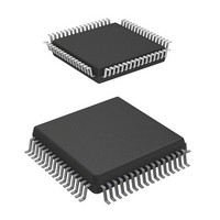
HD64F3644H Renesas Electronics America, HD64F3644H Datasheet - Page 154

HD64F3644H
Manufacturer Part Number
HD64F3644H
Description
IC H8 MCU FLASH 32K 64-QFP
Manufacturer
Renesas Electronics America
Series
H8® H8/300Lr
Datasheet
1.HD64F3644HV.pdf
(551 pages)
Specifications of HD64F3644H
Core Processor
H8/300L
Core Size
8-Bit
Speed
8MHz
Connectivity
SCI
Peripherals
PWM, WDT
Number Of I /o
53
Program Memory Size
32KB (32K x 8)
Program Memory Type
FLASH
Ram Size
1K x 8
Voltage - Supply (vcc/vdd)
2.7 V ~ 5.5 V
Data Converters
A/D 8x8b
Oscillator Type
Internal
Operating Temperature
-20°C ~ 75°C
Package / Case
64-QFP
Package
64PQFP
Family Name
H8
Maximum Speed
8 MHz
Operating Supply Voltage
3.3|5 V
Data Bus Width
8 Bit
Number Of Programmable I/os
45
Interface Type
SCI
On-chip Adc
8-chx8-bit
Number Of Timers
4
Lead Free Status / RoHS Status
Contains lead / RoHS non-compliant
Eeprom Size
-
Available stocks
Company
Part Number
Manufacturer
Quantity
Price
Company:
Part Number:
HD64F3644H
Manufacturer:
HITACHI
Quantity:
490
Company:
Part Number:
HD64F3644H
Manufacturer:
Renesas Electronics America
Quantity:
10 000
Part Number:
HD64F3644H
Manufacturer:
HD
Quantity:
20 000
Company:
Part Number:
HD64F3644HV
Manufacturer:
Renesas
Quantity:
600
Company:
Part Number:
HD64F3644HV
Manufacturer:
Renesas Electronics America
Quantity:
10 000
Part Number:
HD64F3644HV
Manufacturer:
RENESAS/瑞萨
Quantity:
20 000
Part Number:
HD64F3644HV/H83644
Manufacturer:
RENESAS/瑞萨
Quantity:
20 000
- Current page: 154 of 551
- Download datasheet (4Mb)
Section 6 ROM
6.7.4
To erase the flash memory, follow the erasing algorithm shown in figure 6.14. This erasing
algorithm enables data to be erased without subjecting the device to voltage stress or impairing the
reliability of the programmed data.
To erase flash memory, before starting to erase, first place all memory data in all blocks to be
erased in the programmed state (program all memory data to H'00). If all memory data is not in the
programmed state, follow the sequence described later to program the memory data to zero. Select
the flash memory areas to be programmed with erase block registers 1 and 2 (EBR1, EBR2). Next
set the E bit in FLMCR, selecting erase mode. The erase time is the time during which the E bit is
set. To prevent overerasing, use a software timer to divide the time for one erasure, and insure that
the total time does not exceed 30 s. See section 6.7.6, Erase Flowcharts and Sample Programs, for
the time for one erasure. Overerasing, due to program runaway for example, can give memory
cells a negative threshold voltage and cause them to operate incorrectly. Before selecting erase
mode, set up the watchdog timer so as to prevent overerasing.
6.7.5
In erase-verify mode, after data has been erased, it is read to check that it has been erased
correctly. After the erase time has elapsed, exit erase mode (clear the E bit to 0), and select erase-
verify mode (set the EV bit to 1). Before reading data in erase-verify mode, write H'FF dummy
data to the address to be read. This dummy write applies an erase-verify voltage to the memory
cells at the latched address. If the flash memory is read in this state, the data at the latched address
will be read. After the dummy write, wait at least 2 µs before reading. Also, wait at least 4 µs
before performing the first dummy write after selecting erase-verify mode. If the read data has
been successfully erased, perform the erase-verify sequence (dummy write, wait of at least 2 µs,
read) on the next address. If the read data has not been erased, select erase mode again and repeat
the same erase and erase-verify sequence through the last address, until all memory data has been
erased to 1. Do not repeat the erase and erase-verify sequence more than 602 times, however.
Rev. 6.00 Sep 12, 2006 page 132 of 526
REJ09B0326-0600
Erase Mode
Erase-Verify Mode
Related parts for HD64F3644H
Image
Part Number
Description
Manufacturer
Datasheet
Request
R

Part Number:
Description:
(HD64 Series) Hitachi Single-Chip Microcomputer
Manufacturer:
Hitachi Semiconductor
Datasheet:

Part Number:
Description:
KIT STARTER FOR M16C/29
Manufacturer:
Renesas Electronics America
Datasheet:

Part Number:
Description:
KIT STARTER FOR R8C/2D
Manufacturer:
Renesas Electronics America
Datasheet:

Part Number:
Description:
R0K33062P STARTER KIT
Manufacturer:
Renesas Electronics America
Datasheet:

Part Number:
Description:
KIT STARTER FOR R8C/23 E8A
Manufacturer:
Renesas Electronics America
Datasheet:

Part Number:
Description:
KIT STARTER FOR R8C/25
Manufacturer:
Renesas Electronics America
Datasheet:

Part Number:
Description:
KIT STARTER H8S2456 SHARPE DSPLY
Manufacturer:
Renesas Electronics America
Datasheet:

Part Number:
Description:
KIT STARTER FOR R8C38C
Manufacturer:
Renesas Electronics America
Datasheet:

Part Number:
Description:
KIT STARTER FOR R8C35C
Manufacturer:
Renesas Electronics America
Datasheet:

Part Number:
Description:
KIT STARTER FOR R8CL3AC+LCD APPS
Manufacturer:
Renesas Electronics America
Datasheet:

Part Number:
Description:
KIT STARTER FOR RX610
Manufacturer:
Renesas Electronics America
Datasheet:

Part Number:
Description:
KIT STARTER FOR R32C/118
Manufacturer:
Renesas Electronics America
Datasheet:

Part Number:
Description:
KIT DEV RSK-R8C/26-29
Manufacturer:
Renesas Electronics America
Datasheet:

Part Number:
Description:
KIT STARTER FOR SH7124
Manufacturer:
Renesas Electronics America
Datasheet:

Part Number:
Description:
KIT STARTER FOR H8SX/1622
Manufacturer:
Renesas Electronics America
Datasheet:


