Z8F16800144ZCOG Zilog, Z8F16800144ZCOG Datasheet - Page 125
Z8F16800144ZCOG
Manufacturer Part Number
Z8F16800144ZCOG
Description
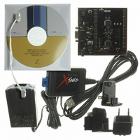
KIT DEV FOR Z8F642 MCU 44 PIN
Manufacturer
Zilog
Series
Z8 Encore!®r
Type
MCUr
Specifications of Z8F16800144ZCOG
Contents
Hardware, Software and Documentation
For Use With/related Products
Z8F642
For Use With
269-4661 - KIT ACC ETHERNET SMART CABLE
Lead Free Status / RoHS Status
Lead free / RoHS Compliant
Other names
269-4678


Table 61. Timer 0–2 Control 1 Register (TxCTL1)
PS025011-1010
BITS
FIELD
RESET
R/W
ADDR
TEN
R/W
7
0
CSC—Cascade Timers
0 = Timer Input signal comes from the pin.
1 = For Timer 0, Input signal is connected to Timer 2 output.
PWMD—PWM Delay Value
This field is a programmable delay to control the number of timer clock cycles time delay
before the Timer Output and the Timer Output Complement is forced to their active state.
000 = No delay
001 = 2 cycles delay
010 = 4 cycles delay
011 = 8 cycles delay
100 = 16 cycles delay
101 = 32 cycles delay
110 = 64 cycles delay
111 = 128 cycles delay
INPCAP—Input Capture Event
This bit indicates if the last timer interrupt is due to a Timer Input Capture Event.
0 = Previous timer interrupt is not a result of Timer Input Capture Event
1 = Previous timer interrupt is a result of Timer Input Capture Event
Timer 0–2 Control 1 Register
The Timer 0–2 Control 1 (TxCTL1) registers enable/disable the timers, set the prescaler
value, and determine the timer operating mode.
TEN—Timer Enable
0 = Timer is disabled.
1 = Timer enabled to count.
TPOL—Timer Input/Output Polarity
Operation of this field is a function of the current operating modes of the timer.
For Timer 1, Input signal is connected to Timer 0 output.
For Timer 2, Input signal is connected to Timer 1 output.
TPOL
R/W
6
0
R/W
5
0
P R E L I M I N A R Y
F07H, F0FH, F17H
PRES
R/W
4
0
R/W
3
0
Z8 Encore! XP
R/W
2
0
Product Specification
TMODE
R/W
1
0
®
F1680 Series
R/W
0
0
Timers
111
Related parts for Z8F16800144ZCOG
Image
Part Number
Description
Manufacturer
Datasheet
Request
R

Part Number:
Description:
Communication Controllers, ZILOG INTELLIGENT PERIPHERAL CONTROLLER (ZIP)
Manufacturer:
Zilog, Inc.
Datasheet:

Part Number:
Description:
KIT DEV FOR Z8 ENCORE 16K TO 64K
Manufacturer:
Zilog
Datasheet:

Part Number:
Description:
KIT DEV Z8 ENCORE XP 28-PIN
Manufacturer:
Zilog
Datasheet:

Part Number:
Description:
DEV KIT FOR Z8 ENCORE 8K/4K
Manufacturer:
Zilog
Datasheet:

Part Number:
Description:
KIT DEV Z8 ENCORE XP 28-PIN
Manufacturer:
Zilog
Datasheet:

Part Number:
Description:
DEV KIT FOR Z8 ENCORE 4K TO 8K
Manufacturer:
Zilog
Datasheet:
Part Number:
Description:
CMOS Z8 microcontroller. ROM 16 Kbytes, RAM 256 bytes, speed 16 MHz, 32 lines I/O, 3.0V to 5.5V
Manufacturer:
Zilog, Inc.
Datasheet:
Part Number:
Description:
Low-cost microcontroller. 512 bytes ROM, 61 bytes RAM, 8 MHz
Manufacturer:
Zilog, Inc.
Datasheet:
Part Number:
Description:
Z8 4K OTP Microcontroller
Manufacturer:
Zilog, Inc.
Datasheet:
Part Number:
Description:
CMOS SUPER8 ROMLESS MCU
Manufacturer:
Zilog, Inc.
Datasheet:
Part Number:
Description:
SL1866 CMOSZ8 OTP Microcontroller
Manufacturer:
Zilog, Inc.
Datasheet:
Part Number:
Description:
SL1866 CMOSZ8 OTP Microcontroller
Manufacturer:
Zilog, Inc.
Datasheet:
Part Number:
Description:
OTP (KB) = 1, RAM = 125, Speed = 12, I/O = 14, 8-bit Timers = 2, Comm Interfaces Other Features = Por, LV Protect, Voltage = 4.5-5.5V
Manufacturer:
Zilog, Inc.
Datasheet:
Part Number:
Description:
Manufacturer:
Zilog, Inc.
Datasheet: