Z8F16800144ZCOG Zilog, Z8F16800144ZCOG Datasheet - Page 274
Z8F16800144ZCOG
Manufacturer Part Number
Z8F16800144ZCOG
Description
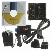
KIT DEV FOR Z8F642 MCU 44 PIN
Manufacturer
Zilog
Series
Z8 Encore!®r
Type
MCUr
Specifications of Z8F16800144ZCOG
Contents
Hardware, Software and Documentation
For Use With/related Products
Z8F642
For Use With
269-4661 - KIT ACC ETHERNET SMART CABLE
Lead Free Status / RoHS Status
Lead free / RoHS Compliant
Other names
269-4678


PS025011-1010
Caution:
Page Erase
Mass Erase
Flash Controller Bypass
Byte Programming can be accomplished using the On-Chip Debugger's Write Memory
command or eZ8 CPU execution of the LDC or LDCI instructions. For a description of the
LDC and LDCI instructions, refer to eZ8 CPU User Manual (UM0128) available for
download at www.zilog.com. While the Flash Controller programs the Flash memory, the
eZ8 CPU idles but the system clock and on-chip peripherals continue to operate. To exit
programming mode and lock the Flash, write any value to the Flash Control register,
except the Mass Erase or Page Erase commands.
The Flash memory can be erased one page (512 bytes) at a time. Page Erasing the Flash
memory sets all bytes in that page to the value
identifies the page to be erased. Only a page residing in an unprotected sector can be
erased. With the Flash Controller unlocked and the active page set, writing the value
to the Flash Control register initiates the Page Erase operation. While the Flash Controller
executes the Page Erase operation, the eZ8 CPU idles but the system clock and on-chip
peripherals continue to operate. The eZ8 CPU resumes operation after the Page Erase
operation completes. If the Page Erase operation is performed using the OCD, poll the
Flash Status register to determine when the Page Erase operation is complete. When the
Page Erase is complete, the Flash Controller returns to its locked state.
The Flash memory can also be Mass Erased using the Flash Controller, but only by using
the On-Chip Debugger. Mass Erasing the Flash memory sets all bytes to the value
With the Flash Controller unlocked and the Mass Erase successfully enabled, writing the
value
Controller executes the Mass Erase operation, the eZ8 CPU idles but the system clock and
on-chip peripherals continue to operate. Using the On-Chip Debugger, poll the Flash
Status register to determine when the Mass Erase operation is complete. When the Mass
Erase is complete, the Flash Controller returns to its locked state.
The Flash Controller can be bypassed and the control signals for the Flash memory is
brought out to the GPIO pins. Bypassing the Flash Controller allows faster Row
Programming algorithms by controlling the Flash programming signals directly.
Row programming is recommended for gang programming applications and large volume
customers who do not require in-circuit initial programming of the Flash memory. Mass
Erase and Page Erase operations are also supported when the Flash Controller is bypassed.
The byte at each address of the Flash memory cannot be programmed (any bits written
to 0) more than twice before an erase cycle occurs.
63H
to the Flash Control register initiates the Mass Erase operation. While the Flash
P R E L I M I N A R Y
FFH
. The Flash Page Select register
Z8 Encore! XP
Product Specification
®
F1680 Series
Flash Memory
FFH
95h
.
260
Related parts for Z8F16800144ZCOG
Image
Part Number
Description
Manufacturer
Datasheet
Request
R

Part Number:
Description:
Communication Controllers, ZILOG INTELLIGENT PERIPHERAL CONTROLLER (ZIP)
Manufacturer:
Zilog, Inc.
Datasheet:

Part Number:
Description:
KIT DEV FOR Z8 ENCORE 16K TO 64K
Manufacturer:
Zilog
Datasheet:

Part Number:
Description:
KIT DEV Z8 ENCORE XP 28-PIN
Manufacturer:
Zilog
Datasheet:

Part Number:
Description:
DEV KIT FOR Z8 ENCORE 8K/4K
Manufacturer:
Zilog
Datasheet:

Part Number:
Description:
KIT DEV Z8 ENCORE XP 28-PIN
Manufacturer:
Zilog
Datasheet:

Part Number:
Description:
DEV KIT FOR Z8 ENCORE 4K TO 8K
Manufacturer:
Zilog
Datasheet:
Part Number:
Description:
CMOS Z8 microcontroller. ROM 16 Kbytes, RAM 256 bytes, speed 16 MHz, 32 lines I/O, 3.0V to 5.5V
Manufacturer:
Zilog, Inc.
Datasheet:
Part Number:
Description:
Low-cost microcontroller. 512 bytes ROM, 61 bytes RAM, 8 MHz
Manufacturer:
Zilog, Inc.
Datasheet:
Part Number:
Description:
Z8 4K OTP Microcontroller
Manufacturer:
Zilog, Inc.
Datasheet:
Part Number:
Description:
CMOS SUPER8 ROMLESS MCU
Manufacturer:
Zilog, Inc.
Datasheet:
Part Number:
Description:
SL1866 CMOSZ8 OTP Microcontroller
Manufacturer:
Zilog, Inc.
Datasheet:
Part Number:
Description:
SL1866 CMOSZ8 OTP Microcontroller
Manufacturer:
Zilog, Inc.
Datasheet:
Part Number:
Description:
OTP (KB) = 1, RAM = 125, Speed = 12, I/O = 14, 8-bit Timers = 2, Comm Interfaces Other Features = Por, LV Protect, Voltage = 4.5-5.5V
Manufacturer:
Zilog, Inc.
Datasheet:
Part Number:
Description:
Manufacturer:
Zilog, Inc.
Datasheet: