Z8F16800144ZCOG Zilog, Z8F16800144ZCOG Datasheet - Page 208
Z8F16800144ZCOG
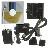
Manufacturer Part Number
Z8F16800144ZCOG
Description
KIT DEV FOR Z8F642 MCU 44 PIN
Manufacturer
Zilog
Series
Z8 Encore!®r
Type
MCUr
Specifications of Z8F16800144ZCOG
Contents
Hardware, Software and Documentation
For Use With/related Products
Z8F642
For Use With
269-4661 - KIT ACC ETHERNET SMART CABLE
Lead Free Status / RoHS Status
Lead free / RoHS Compliant
Other names
269-4678


ESPI Register Overview
Operation
PS025011-1010
Slave Select
The Slave Select signal is a bidirectional framing signal with several modes of operation
to support SPI and other synchronous serial interface protocols. The Slave Select mode is
selected by the SSMD field of the ESPI Mode register. The direction of the SS signal is
controlled by the SSIO bit of the ESPI Mode register. The SS signal is an input on slave
devices and is an output on the active Master device. Slave devices ignore transactions on
the bus unless their Slave Select input is asserted. In SPI MASTER mode, additional
GPIO pins are required to provide Slave Selects if there is more than one slave device.
The ESPI Control/Status Registers are summarized in
During a transfer, data is sent and received simultaneously by both the Master and Slave
devices. Separate signals are required for transmit data, receive data, and the serial clock.
When a transfer occurs, a multi-bit (typically 8-bit) character is shifted out one data pin
and a multi-bit character is simultaneously shifted in on second data pin. An 8-bit shift
register in the Master and an 8-bit shift register in the Slave are connected as a circular
buffer. The ESPI shift register is buffered to support back-to-back character transfers in
high performance applications.
A transaction is initiated when the Data register is written in the Master device. The value
from the Data register is transferred into the shift register and the I2C transaction begins.
At the end of each character transfer, if the next transmit value has been written to the data
register, the data and shift register values are swapped, which places the new transmit data
into the shift register and the shift register contents (receive data) into the data register. At
that point the Receive Data Register Not Empty signal is asserted (RDRNE bit set in the
Status Register). Once software reads the receive data from the Data register, the Transmit
Data Register Empty signal is asserted (TDRE bit set in the Status Register) to request the
next transmit byte. To support back-to-back transfers without an intervening pause, the
receive and transmit interrupts must be serviced when the current character is being
transferred.
Table 108. ESPI Registers
Address
XX0
XX2
XX4
XX6
Even Address
Data
Control
Status
Baud Rate High Baud Rate Low
P R E L I M I N A R Y
Odd Address
Transmit Data Command and Receive Date Buffer Control
Mode
State
Table 108.
Z8 Encore! XP
Enhanced Serial Peripheral Interface
Product Specification
®
F1680 Series
194
Related parts for Z8F16800144ZCOG
Image
Part Number
Description
Manufacturer
Datasheet
Request
R

Part Number:
Description:
Communication Controllers, ZILOG INTELLIGENT PERIPHERAL CONTROLLER (ZIP)
Manufacturer:
Zilog, Inc.
Datasheet:

Part Number:
Description:
KIT DEV FOR Z8 ENCORE 16K TO 64K
Manufacturer:
Zilog
Datasheet:

Part Number:
Description:
KIT DEV Z8 ENCORE XP 28-PIN
Manufacturer:
Zilog
Datasheet:

Part Number:
Description:
DEV KIT FOR Z8 ENCORE 8K/4K
Manufacturer:
Zilog
Datasheet:

Part Number:
Description:
KIT DEV Z8 ENCORE XP 28-PIN
Manufacturer:
Zilog
Datasheet:

Part Number:
Description:
DEV KIT FOR Z8 ENCORE 4K TO 8K
Manufacturer:
Zilog
Datasheet:
Part Number:
Description:
CMOS Z8 microcontroller. ROM 16 Kbytes, RAM 256 bytes, speed 16 MHz, 32 lines I/O, 3.0V to 5.5V
Manufacturer:
Zilog, Inc.
Datasheet:
Part Number:
Description:
Low-cost microcontroller. 512 bytes ROM, 61 bytes RAM, 8 MHz
Manufacturer:
Zilog, Inc.
Datasheet:
Part Number:
Description:
Z8 4K OTP Microcontroller
Manufacturer:
Zilog, Inc.
Datasheet:
Part Number:
Description:
CMOS SUPER8 ROMLESS MCU
Manufacturer:
Zilog, Inc.
Datasheet:
Part Number:
Description:
SL1866 CMOSZ8 OTP Microcontroller
Manufacturer:
Zilog, Inc.
Datasheet:
Part Number:
Description:
SL1866 CMOSZ8 OTP Microcontroller
Manufacturer:
Zilog, Inc.
Datasheet:
Part Number:
Description:
OTP (KB) = 1, RAM = 125, Speed = 12, I/O = 14, 8-bit Timers = 2, Comm Interfaces Other Features = Por, LV Protect, Voltage = 4.5-5.5V
Manufacturer:
Zilog, Inc.
Datasheet:
Part Number:
Description:
Manufacturer:
Zilog, Inc.
Datasheet: