Z8F16800144ZCOG Zilog, Z8F16800144ZCOG Datasheet - Page 273
Z8F16800144ZCOG
Manufacturer Part Number
Z8F16800144ZCOG
Description
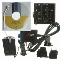
KIT DEV FOR Z8F642 MCU 44 PIN
Manufacturer
Zilog
Series
Z8 Encore!®r
Type
MCUr
Specifications of Z8F16800144ZCOG
Contents
Hardware, Software and Documentation
For Use With/related Products
Z8F642
For Use With
269-4661 - KIT ACC ETHERNET SMART CABLE
Lead Free Status / RoHS Status
Lead free / RoHS Compliant
Other names
269-4678


PS025011-1010
Byte Programming
Flash Code Protection Using the Flash Controller
At Reset, the Flash Controller locks to prevent accidental program or erasure of the Flash
memory. To program or erase the Flash memory, first write the Page Select Register with
the target page. Unlock the Flash Controller by making two consecutive writes to the
Flash Control register with the values
must be rewritten with the same page previously stored there. If the two Page Select writes
do not match, the controller reverts to a locked state. If the two writes match, the selected
page becomes active. For details, see
After unlocking a specific page, you can either enable Page Program or Erase. Writing
the value
protected. Any other value written to the Flash Control register locks the Flash Controller.
Mass Erase is not allowed in the user code but only in through the Debug Port.
After unlocking a specific page, you can also write to any byte on that page. After a byte is
written, the page remains unlocked, allowing for subsequent writes to other bytes on the
same page. Further writes to the Flash Control Register cause the active page to revert to a
locked state.
Sector Based Flash Protection
The final protection mechanism is implemented on a per-sector basis. The Flash memories
of Z8 Encore! devices are divided into a maximum number of 8 sectors. A sector is 1/8 of
the total size of the Flash memory unless this value is smaller than the page size, in which
case the sector and page sizes are equal. On the Z8 Encore! XP F1680 Series devices, the
sector size is 3 KB, 2 KB or 1 KB depending on available on-chip Flash size of 24 KB, 16
KB, and 8 KB.
The Sector Protect Register controls the protection state of each Flash sector. This register
is shared with the Page Select Register. This is accessed by unlocking the Flash controller
and writing the command byte
Sector Protect Register.
The Sector Protect Register is initialized to 0 on Reset, putting each sector into an
unprotected state. When a bit in the Sector Protect Register is written to 1, the
corresponding sector can no longer be written or erased. After a bit of the Sector Protect
Register has been set, it can not be cleared except by powering down the device.
The Flash memory is enabled for byte programming after unlocking the Flash Controller
and successfully enabling either Mass Erase or Page Erase. When the Flash Controller is
unlocked and Mass Erase is successfully enabled, all Program Memory locations are
available for byte programming. In contrast, when the Flash Controller is unlocked and
Page Erase is successfully enabled, only the locations of the selected page are available for
byte programming. An erased Flash byte contains all 1’s (
operation can only be used to change bits from 1 to 0. To change a Flash bit (or multiple
bits) from 0 to 1 requires execution of either the Page Erase or Mass Erase commands.
95H
causes a Page Erase, only if the active page resides in a sector that is not
P R E L I M I N A R Y
5EH
. The next write to the Page Select Register targets the
73H
Figure 54
and
8CH
on page 257.
, sequentially. The Page Select Register
Z8 Encore! XP
FFH
). The programming
Product Specification
®
F1680 Series
Flash Memory
259
Related parts for Z8F16800144ZCOG
Image
Part Number
Description
Manufacturer
Datasheet
Request
R

Part Number:
Description:
Communication Controllers, ZILOG INTELLIGENT PERIPHERAL CONTROLLER (ZIP)
Manufacturer:
Zilog, Inc.
Datasheet:

Part Number:
Description:
KIT DEV FOR Z8 ENCORE 16K TO 64K
Manufacturer:
Zilog
Datasheet:

Part Number:
Description:
KIT DEV Z8 ENCORE XP 28-PIN
Manufacturer:
Zilog
Datasheet:

Part Number:
Description:
DEV KIT FOR Z8 ENCORE 8K/4K
Manufacturer:
Zilog
Datasheet:

Part Number:
Description:
KIT DEV Z8 ENCORE XP 28-PIN
Manufacturer:
Zilog
Datasheet:

Part Number:
Description:
DEV KIT FOR Z8 ENCORE 4K TO 8K
Manufacturer:
Zilog
Datasheet:
Part Number:
Description:
CMOS Z8 microcontroller. ROM 16 Kbytes, RAM 256 bytes, speed 16 MHz, 32 lines I/O, 3.0V to 5.5V
Manufacturer:
Zilog, Inc.
Datasheet:
Part Number:
Description:
Low-cost microcontroller. 512 bytes ROM, 61 bytes RAM, 8 MHz
Manufacturer:
Zilog, Inc.
Datasheet:
Part Number:
Description:
Z8 4K OTP Microcontroller
Manufacturer:
Zilog, Inc.
Datasheet:
Part Number:
Description:
CMOS SUPER8 ROMLESS MCU
Manufacturer:
Zilog, Inc.
Datasheet:
Part Number:
Description:
SL1866 CMOSZ8 OTP Microcontroller
Manufacturer:
Zilog, Inc.
Datasheet:
Part Number:
Description:
SL1866 CMOSZ8 OTP Microcontroller
Manufacturer:
Zilog, Inc.
Datasheet:
Part Number:
Description:
OTP (KB) = 1, RAM = 125, Speed = 12, I/O = 14, 8-bit Timers = 2, Comm Interfaces Other Features = Por, LV Protect, Voltage = 4.5-5.5V
Manufacturer:
Zilog, Inc.
Datasheet:
Part Number:
Description:
Manufacturer:
Zilog, Inc.
Datasheet: