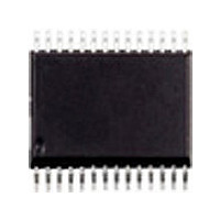
ST52F513G3M6 STMicroelectronics, ST52F513G3M6 Datasheet - Page 103

ST52F513G3M6
Manufacturer Part Number
ST52F513G3M6
Description
Manufacturer
STMicroelectronics
Datasheet
1.ST52F513G3M6.pdf
(136 pages)
Specifications of ST52F513G3M6
Cpu Family
ST52
Device Core Size
8b
Frequency (max)
20MHz
Interface Type
I2C/SCI/SPI
Program Memory Type
Flash
Program Memory Size
8KB
Total Internal Ram Size
256Byte
# I/os (max)
22
Number Of Timers - General Purpose
2
Operating Supply Voltage (typ)
3.3/5V
Operating Supply Voltage (max)
5.5V
Operating Supply Voltage (min)
2.7V
On-chip Adc
8-chx10-bit
Instruction Set Architecture
CISC
Operating Temp Range
-40C to 85C
Operating Temperature Classification
Industrial
Mounting
Surface Mount
Pin Count
28
Package Type
SO
Lead Free Status / Rohs Status
Compliant
Available stocks
Company
Part Number
Manufacturer
Quantity
Price
Part Number:
ST52F513G3M6
Manufacturer:
ST
Quantity:
20 000
Part Number:
ST52F513G3M6TR
Manufacturer:
ST
Quantity:
20 000
Figure 15.5 Clearing the WCOL bit (Write Collision Flag) Software Sequence
15.4.6 Overrun Condition.
An overrun condition occurs when the master
device has sent several data bytes and the slave
device hasn’t cleared the SPIF bit issued from the
previous data byte transmitted.
In this case, the receiver buffer contains the byte
sent after the SPIF bit was last cleared. A read to
the SPI_IN register returns this byte. All other
bytes are lost.
This condition is not detected by the SPI
peripheral.
15.4.7 Single Master and Multimaster Configu-
rations.
There are two types of SPI systems:
– Single Master System
– Multimaster System
Single Master System
A typical single master system may be configured,
using an ICU as the master and four ICUs as
slaves see
The master device selects the individual slave
devices by using four pins of a parallel port to
control the four SS pins of the slave devices.
The SS pins are pulled high during reset since the
master device ports will be forced to be inputs at
that time, thus disabling the slave devices.
Note: In order to prevent a bus conflict on the
MISO line the master allows only one active slave
device during a transmission.
1st Step
2nd Step
Clearing sequence after SPIF = 1 (end of a data byte transfer)
Clearing sequence before SPIF = 1 (during a data byte transfer)
1st Step
2nd Step
(Figure
Read SPI_STATUS_CR
Read SPI_IN
15.6).
THEN
SPIF =0
WCOL=0
Read SPI_IN
Read SPI_STATUS_CR
OR
THEN
Read SPI_STATUS_CR
Write SPI_OUT
WCOL=0
For more security, the slave device may respond to
the master with the data byte received. Then the
master will receive the previous byte back from the
slave device if all MISO and MOSI pins are
connected and the slave has not written its
SPI_OUT register.
Other transmission security methods can use ports
for handshake lines or data bytes with command
fields.
Multi-master System
A multi-master system may also be configured by
the user. Transfer of master control could be
implemented using a handshake method through
the I/O ports or by an exchange of code messages
through the serial peripheral interface system.
The multi-master system is principally handled by
the MSTR bit in the SPI_CR register and the
MODF bit in the SPI_STATUS_CR register.
Note: Writing in SPI_OUT regis-
ter instead of reading in SPI_IN
do not reset WCOL bit
THEN
SPIF =0
WCOL=0
WCOL=1
before the 2nd step
ST52510xx ST52513xx
if no transfer has started
if a transfer has started
103/136


