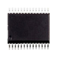
ST52F513G3M6 STMicroelectronics, ST52F513G3M6 Datasheet - Page 89

ST52F513G3M6
Manufacturer Part Number
ST52F513G3M6
Description
Manufacturer
STMicroelectronics
Datasheet
1.ST52F513G3M6.pdf
(136 pages)
Specifications of ST52F513G3M6
Cpu Family
ST52
Device Core Size
8b
Frequency (max)
20MHz
Interface Type
I2C/SCI/SPI
Program Memory Type
Flash
Program Memory Size
8KB
Total Internal Ram Size
256Byte
# I/os (max)
22
Number Of Timers - General Purpose
2
Operating Supply Voltage (typ)
3.3/5V
Operating Supply Voltage (max)
5.5V
Operating Supply Voltage (min)
2.7V
On-chip Adc
8-chx10-bit
Instruction Set Architecture
CISC
Operating Temp Range
-40C to 85C
Operating Temperature Classification
Industrial
Mounting
Surface Mount
Pin Count
28
Package Type
SO
Lead Free Status / Rohs Status
Compliant
Available stocks
Company
Part Number
Manufacturer
Quantity
Price
Part Number:
ST52F513G3M6
Manufacturer:
ST
Quantity:
20 000
Part Number:
ST52F513G3M6TR
Manufacturer:
ST
Quantity:
20 000
Acknowledge may be enabled and disabled via
software.
The I
address can be selected via software.
The speed of the I
between Standard (0-100KHz) and Fast I
400KHz).
14.3.3 SDA/SCL Line Control.
Transmitter mode: the interface holds the clock line
low before transmission, in order to wait for the
microcontroller to write the byte in the Data
Register.
Receiver mode: the interface holds the clock line
low after reception to wait for the microcontroller to
read the byte in the Data Register.
SCL frequency is controlled by a programmable
clock divider which depends on the I
Figure 14.2 I
SDA
SCL
2
C interface address and/or general call
SDA
SCL
2
C Interface Block Diagram
2
C interface may be selected
CLOCK CONTROL REGISTER (I2C_CCR)
CLOCK CONTROL
STATUS REGISTER 1 (I2C_SR1)
STATUS REGISTER 2 (I2C_SR2)
CONTROL REGISTER (I2C_CR)
DATA CONTROL
2
C bus mode.
2
C (100-
When the I
pins must be configured as open-drain with or
without pull-up. The value of the external pull-up
resistance used depends on the application.
14.4 Functional Description
By default the I
mode (M/SL bit is cleared) except when it initiates
a transmit or receive sequence.
First, the interface frequency must be configured
using the related bits of the Configuration
Registers.
14.4.1 Slave Mode.
As soon as a start condition is detected, the
address is received from the SDA line and sent to
the shift register; then it is compared with the
address of the interface or the General Call
address (if selected by software).
OWN ADDRESS REGISTER (OAR)
DATA SHIFT REGISTER
2
CONTROL LOGIC
DATA REGISTER
C cell is enabled, the SDA and SCL
COMPARATOR
INTERRUPT
2
C interface operates in Slave
ST52510xx ST52513xx
89/136


