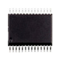
ST52F513G3M6 STMicroelectronics, ST52F513G3M6 Datasheet - Page 8

ST52F513G3M6
Manufacturer Part Number
ST52F513G3M6
Description
Manufacturer
STMicroelectronics
Datasheet
1.ST52F513G3M6.pdf
(136 pages)
Specifications of ST52F513G3M6
Cpu Family
ST52
Device Core Size
8b
Frequency (max)
20MHz
Interface Type
I2C/SCI/SPI
Program Memory Type
Flash
Program Memory Size
8KB
Total Internal Ram Size
256Byte
# I/os (max)
22
Number Of Timers - General Purpose
2
Operating Supply Voltage (typ)
3.3/5V
Operating Supply Voltage (max)
5.5V
Operating Supply Voltage (min)
2.7V
On-chip Adc
8-chx10-bit
Instruction Set Architecture
CISC
Operating Temp Range
-40C to 85C
Operating Temperature Classification
Industrial
Mounting
Surface Mount
Pin Count
28
Package Type
SO
Lead Free Status / Rohs Status
Compliant
Available stocks
Company
Part Number
Manufacturer
Quantity
Price
Part Number:
ST52F513G3M6
Manufacturer:
ST
Quantity:
20 000
Part Number:
ST52F513G3M6TR
Manufacturer:
ST
Quantity:
20 000
ST52510xx ST52513xx
configuration registers, in order to avoid overlap
with other data.
Single Voltage Flash allows the user to reprogram
the devices on-board by means of the In Situ
Programming (ISP) feature. It is possible to store in
safe way up to 4K of data in the available EEPROM
memory benches. Permanent data, both in Flash
and EEPROM can be managed by means of the
In-Application-Programming (IAP) feature. Single
byte and Page write modes are supported. Flexible
write protection, of permanent data or program
instructions, is also available.
The Instruction Set composed of up to 107
instructions allows code compression and high
speed in the program implementation.
A powerful development environment consisting of
a board and software tools allows an easy
configuration and use of ST52510/513.
T h e V i s u a l F I V E s o f t w a r e t o o l a l l o w s t h e
development and debugging of projects via a user-
friendly graphical interface and optimization of
generated microcode.
Third-party Hardware Emulators and ‘C’ Compiler
a r e a v a i l a b l e t o s pe e d- u p t he a p pl i c at i o n
implementation and time-to-market.
1.2 Functional Description
ST52510/513 ICU’s can work in two modes
according to the Vpp signal levels:
■
■
During Working Mode Vpp must be tied to Vss. To
enter the Memory Programming Mode, the Vpp pin
must be tied to Vdd.
A RESET signal must be applied to the device to
switch from one mode to the other.
1.2.1 Memory Programming Mode.
The ST52510/513 memory is loaded in the
Memory Programming Mode. All instructions and
data are written inside the memory during this
phase. The user Option Bytes are loaded during
this phase by using the programming tools. The
8/136
Memory Programming Mode
Working Mode
Option Bytes can only be loaded in this phase and
cannot be modified run-time.
Data and commands are transmitted by using the
I
peripheral. The In-Situ Programming protocol
(ISP) uses the following pins:
■
■
■
■
The Internal clock is used in this phase.
1.2.2 Working Mode.
The processor starts the working phase following
the instructions, which have been previously
loaded in the first locations of the memory. The first
instruction must be a jump to the first program
instruction, skipping the data (interrupt vectors,
Membership Functions, user data) stored in the
first memory page.
ST52510/513’s internal structure includes two
computational blocks, the CONTROL UNIT (CU)
and the DATA PROCESSING UNIT (DPU), which
performs boolean functions. The DECISION
PROCESSOR (DP) block cooperates with these
blocks to perform Fuzzy algorithms.
The DP can manage up to 340 different
Membership Functions for the antecedent part of
fuzzy rules. The consequent terms of the rules are
“crisp” values (real numbers). The maximum
number of rules that can be defined is limited by
the
implemented.
The Program/Data Memory is shared between
Fuzzy and standard algorithms. Within this
memory, the user data can be stored both in non
volatile memory as well as in the RAM locations.
The Control Unit (CU) reads information and the
status of the peripherals.
Arithmetic calculus can be performed on these
values by using the internal CU and Register File,
which supports all computations. The peripheral
inputs can be Fuzzy and/or arithmetic output
values contained in the Register File or Program/
Data Memory.
2
C protocol, implemented using the internal I
SDA and SCL for transmission
Vpp for entering in the mode
RESET for starting the protocol in a stable status
Vdd and Vss for the power supply.
dimensions
of
the
standard
algorithm
2
C


