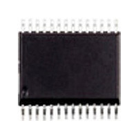
ST52F513G3M6 STMicroelectronics, ST52F513G3M6 Datasheet - Page 33

ST52F513G3M6
Manufacturer Part Number
ST52F513G3M6
Description
Manufacturer
STMicroelectronics
Datasheet
1.ST52F513G3M6.pdf
(136 pages)
Specifications of ST52F513G3M6
Cpu Family
ST52
Device Core Size
8b
Frequency (max)
20MHz
Interface Type
I2C/SCI/SPI
Program Memory Type
Flash
Program Memory Size
8KB
Total Internal Ram Size
256Byte
# I/os (max)
22
Number Of Timers - General Purpose
2
Operating Supply Voltage (typ)
3.3/5V
Operating Supply Voltage (max)
5.5V
Operating Supply Voltage (min)
2.7V
On-chip Adc
8-chx10-bit
Instruction Set Architecture
CISC
Operating Temp Range
-40C to 85C
Operating Temperature Classification
Industrial
Mounting
Surface Mount
Pin Count
28
Package Type
SO
Lead Free Status / Rohs Status
Compliant
Available stocks
Company
Part Number
Manufacturer
Quantity
Price
Part Number:
ST52F513G3M6
Manufacturer:
ST
Quantity:
20 000
Part Number:
ST52F513G3M6TR
Manufacturer:
ST
Quantity:
20 000
4 MEMORY PROGRAMMING
ST52F510/F513
programmable non-volatile memory, which allows
fast and reliable storage of user data.
Program/Data Memory addressing space is
composed by a Single Voltage Flash Memory and
a RAM memory bench. The ST52F513 devices
also have a Data EEPROM bench to store
permanent data with long term retention and a high
number of write/erase cycles.
All the Program Data memory addresses can
execute code, including RAM and EEPROM
benches.
The memory is programmed by setting the V
equal to V
through the I
same procedure is used to perform “In-Situ” the
programming of the device after it is mounted in
the user system. Data can also be written in run-
time with the In-Application Programming (IAP)
instructions.
The Memory can be locked by the user during the
programming phase, in order to prevent external
operation such as reading the program code and
assuring protection of user intellectual property.
Table 4.1 Sales Type Memory Organization
ST52F510c3p6
ST52F513c3p6
legend:
c:
p:
Y=16 pins, F=20 pins, G=28 pins, K=32/34 pin
B=DIP, M=SO, T=TQFP
Device
dd
. Data and commands are transmitted
2
C serial communication protocol. The
provides
8192 bytes
7936 bytes
Amount
Flash Memory
an
on-chip
0 to 31
0 to 30
Pages
pp
user
pin
256 bytes
256 bytes
Amount
Flash and EEPROM pages can be protected by
unintentional writings.
Remark: the memory contents are protected by
the Error Correction Code (ECC) algorithm that
uses a 4-bit redundancy to correct one bit errors.
4.1 Program/Data Memory Organization
The Program/Data Memory is organized as
described in
have different amounts of each type of memory.
Table 4.1
and page allocation for each sales type.
The addressing spaces are organized in pages of
256 bytes. Each page is composed by blocks of 32
bytes. Memory programming is performed one
block at a time in order to speed-up the
programming time (about 2.5 ms per block).
The whole location address is composed as
follows:
RAM Memory
15
Page address
describes the memory benches amount
Page
32
32
Section
3.3. The various sales types
8
ST52510xx ST52513xx
256 bytes
Amount
Block address address inside the block
7
EEPROM Memory
-
5
4
Page(s)
31
-
33/136
0


