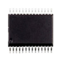
ST52F513G3M6 STMicroelectronics, ST52F513G3M6 Datasheet - Page 94

ST52F513G3M6
Manufacturer Part Number
ST52F513G3M6
Description
Manufacturer
STMicroelectronics
Datasheet
1.ST52F513G3M6.pdf
(136 pages)
Specifications of ST52F513G3M6
Cpu Family
ST52
Device Core Size
8b
Frequency (max)
20MHz
Interface Type
I2C/SCI/SPI
Program Memory Type
Flash
Program Memory Size
8KB
Total Internal Ram Size
256Byte
# I/os (max)
22
Number Of Timers - General Purpose
2
Operating Supply Voltage (typ)
3.3/5V
Operating Supply Voltage (max)
5.5V
Operating Supply Voltage (min)
2.7V
On-chip Adc
8-chx10-bit
Instruction Set Architecture
CISC
Operating Temp Range
-40C to 85C
Operating Temperature Classification
Industrial
Mounting
Surface Mount
Pin Count
28
Package Type
SO
Lead Free Status / Rohs Status
Compliant
Available stocks
Company
Part Number
Manufacturer
Quantity
Price
Part Number:
ST52F513G3M6
Manufacturer:
ST
Quantity:
20 000
Part Number:
ST52F513G3M6TR
Manufacturer:
ST
Quantity:
20 000
ST52510xx ST52513xx
14.5 Register Description
In the following sections describe the registers
used by the I
14.5.1 I
I
Configuration Register 16 (010h) Read/Write
Reset Value: 0000 0000 (00h)
Bit 7-6: Not Used. They must be held to 0.
Bit 5: PE Peripheral Enable.
Notes:
– When PE=0, all the bits of the I2C_CR register
– When PE=1, the corresponding I/O pins are se-
– To enable the I
Bit 4: ENGC Enable General Call
Note:
acknowledged (01h ignored).
Bit 3: START Generation of a Start Condition
94/136
2
C Control Register (I2C_CR)
and the SR register except the Stop bit are reset.
All outputs are released while PE=0
lected by hardware as alternate functions.
register TWICE with PE=1 as the first write only
activates the interface (only PE is set).
7
-
– In Master Mode
This bit is set and cleared by software
0: peripheral disabled
1: peripheral enabled
This bit is set and cleared by software. It is
also cleared by hardware when the interface
is disabled (PE=0).
0: General Call disabled
1: General Call enabled
This bit is set and cleared by software. It is
also cleared by hardware when the interface
is disabled (PE=0) or when the Start
condition is sent (with interrupt generation if
ITE=1).
0: No Start generation
1: Repeated Start generation
2
The
C Interface Configuration Registers.
-
2
C Interface are described.
PE
00h
2
C interface, write the I2C_CR
ENGC
General
START
Call
ACK
address
STOP
ITE
0
is
Bit 2: ACK Acknowledge enable
Bit 1: STOP Generation of a Stop Condition
Bit 0: ITE Interrupt Enable
I
Configuration Register 17 (011h) Read/Write
Reset Value: 0000 0000 (00h)
Bit 7: FM/SM Fast/Standard I
2
FM/SM
C Clock Control Register (I2C_CCR)
7
– In Slave Mode
– In Master Mode
– In Slave Mode
0: No Start generation
1: Start generation when the bus is free
This bit is set and cleared by software. It is
also cleared by hardware when the interface
is disabled (PE=0).
0: No acknowledge returned
1: Acknowledge returned after an address
This bit is set and cleared by software. It is
also cleared by hardware in master mode.
Note: This bit is not cleared when the
interface is disabled (PE=0).
0: No Stop generation
1: Stop generation after the current byte
0: No actions performed
1: Release the SCL and SDA lines after the
0: Interrupt disabled
1: Interrupt enabled
This bit is set and cleared by software. It is
not cleared when the interface is disabled
(PE=0).
CC6
byte or a data byte is received
transfer or after the current Start condition
is sent. The STOP bit is cleared by
hardware when the Stop condition is sent.
last byte transfer (BTF=1) in slave
transmitter mode. In this mode the STOP
bit has to be cleared by software.
CC5
CC4
CC3
2
C Mode.
CC2
CC1
CC0
0


