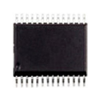
ST52F513G3M6 STMicroelectronics, ST52F513G3M6 Datasheet - Page 99

ST52F513G3M6
Manufacturer Part Number
ST52F513G3M6
Description
Manufacturer
STMicroelectronics
Datasheet
1.ST52F513G3M6.pdf
(136 pages)
Specifications of ST52F513G3M6
Cpu Family
ST52
Device Core Size
8b
Frequency (max)
20MHz
Interface Type
I2C/SCI/SPI
Program Memory Type
Flash
Program Memory Size
8KB
Total Internal Ram Size
256Byte
# I/os (max)
22
Number Of Timers - General Purpose
2
Operating Supply Voltage (typ)
3.3/5V
Operating Supply Voltage (max)
5.5V
Operating Supply Voltage (min)
2.7V
On-chip Adc
8-chx10-bit
Instruction Set Architecture
CISC
Operating Temp Range
-40C to 85C
Operating Temperature Classification
Industrial
Mounting
Surface Mount
Pin Count
28
Package Type
SO
Lead Free Status / Rohs Status
Compliant
Available stocks
Company
Part Number
Manufacturer
Quantity
Price
Part Number:
ST52F513G3M6
Manufacturer:
ST
Quantity:
20 000
Part Number:
ST52F513G3M6TR
Manufacturer:
ST
Quantity:
20 000
Figure 15.2 Serial Peripheral Interface Block Diagram
Procedure
– Select the SPR0, SPR1 and SPR2 bits to define
– Select the CPOL and CPHA bits to define one of
– The SS pin must be connected to a high level
– The MSTR and SPE bits must be set (they re-
In this configuration the MOSI pin is a data output
and to the MISO pin is a data input.
Transmit sequence
Transmit sequence begins when a byte is written in
the SPI_OUT register.
the serial clock baud rate (see SPI_CR register).
the four relationships between the data transfer
and the serial clock (see
signal during the complete byte transmit se-
quence, if this pin is used.
main set only if the SS pin is connected to a high
level signal).
MOSI
MISO
SCK
SS
8-Bit Shift Register
Read
Figure
Read Buffer
Write
15.4).
CONTROL
SERIAL
CLOCK
GENERATOR
MASTER
Internal Bus
SPI_OUT
SPI_IN
The data byte is loaded in parallel into the 8-bit shift
register (from the internal bus) during a write cycle
and then shifted out serially to the MOSI pin most
significant bit first.
When data transfer is complete:
– The SPIF bit is set by hardware
– An interrupt is generated if the SPIE bit is set.
During the last clock cycle the SPIF bit is set, a
copy of the data byte received in the shift register
is moved to a buffer. When the SPI_IN register is
read, the SPI peripheral returns this buffered
value. Clearing the SPIF bit is performed by the
following software sequence:
1. An access to the SPI_STATUS_CR register
2. A read to the SPI_IN register.
Note: While the SPIF bit is set, all writes to the
SPI_OUT
SPI_STATUS_CR register is read.
while the SPIF bit is set
SPIE
SPIF WCOL
SPE
register
CONTROL
SPR2
STATE
SPI
OR
MSTR
are
ST52510xx ST52513xx
MODF
CPOL
inhibited
-
SPI_STATUS_CR
CPHA
SOD
SPR1
SSM
request
until
IT
SPI_CR
SPR0
SSI
99/136
the


