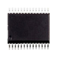
ST52F513G3M6 STMicroelectronics, ST52F513G3M6 Datasheet - Page 7

ST52F513G3M6
Manufacturer Part Number
ST52F513G3M6
Description
Manufacturer
STMicroelectronics
Datasheet
1.ST52F513G3M6.pdf
(136 pages)
Specifications of ST52F513G3M6
Cpu Family
ST52
Device Core Size
8b
Frequency (max)
20MHz
Interface Type
I2C/SCI/SPI
Program Memory Type
Flash
Program Memory Size
8KB
Total Internal Ram Size
256Byte
# I/os (max)
22
Number Of Timers - General Purpose
2
Operating Supply Voltage (typ)
3.3/5V
Operating Supply Voltage (max)
5.5V
Operating Supply Voltage (min)
2.7V
On-chip Adc
8-chx10-bit
Instruction Set Architecture
CISC
Operating Temp Range
-40C to 85C
Operating Temperature Classification
Industrial
Mounting
Surface Mount
Pin Count
28
Package Type
SO
Lead Free Status / Rohs Status
Compliant
Available stocks
Company
Part Number
Manufacturer
Quantity
Price
Part Number:
ST52F513G3M6
Manufacturer:
ST
Quantity:
20 000
Part Number:
ST52F513G3M6TR
Manufacturer:
ST
Quantity:
20 000
1 GENERAL DESCRIPTION
1.1 Introduction
ST52510/513 are devices of ST FIVE family of 8-
bit Intelligent Controller Units (ICU), which can
perform, both boolean and Fuzzy algorithms in an
efficient manner, in order to reach the best
performances that the two methodologies allow.
Produced by STMicroelectronics using the reliable
high performance CMOS process for Single
Voltage Flash versions, ST52510/513 include
integrated
maximization of system reliability, and decreased
system costs in order to minimize the number of
external components.
The flexible I/O configuration of ST52510/513
allow one to interface with a wide range of external
devices (for example D/A converters or power
control devices), and to communicate with the
most common serial standards.
ST52510/513 pins are configurable. The user can
set input or output signals on each single pin in 8
different modes, reducing the need for external
components in order to supply a suitable interface
with the port pins.
A hardware multiplier and divider, together with a
wide instruction set, allow the implementation of
complex functions by using a single instruction.
Therefore,
computational speed is optimized.
Fuzzy Logic dedicated structures in ST52510/513
ICU’s can be exploited to model complex system
with high accuracy in a useful and simple manner.
Fuzzy
management and Fuzzy Real time Controls can be
designed to increase performance at competitive
costs.
The linguistic approach characterizing Fuzzy Logic
is based on a set of IF-THEN rules, which describe
the control behavior and on Membership Functions
associated with input and output variables.
Up to 340 Membership Functions, with triangular
and trapezoidal shapes, or singleton values are
available to describe fuzzy variables.
The Timer/PWM peripheral allows one to manage
power devices and timing signals, by implementing
different operating modes and high frequency
PWM (Pulse Width Modulation) controls. Input
Capture and Output Compare functions are
available on the Timers.
The Timer has a 16-bit programmable internal
Prescaler and a 16-bit Counter, which can use
internal or external START/STOP signals and
clock.
An
available to avoid loop errors and reset the ICU.
internal
Expert
program
on-chip
programmable
Systems
peripherals
memory
for
WATCHDOG
overall
utilization
that
system
allow
and
is
ST52510/513 includes a 10-bit, self-calibrating,
Analog to Digital Converter with an 8-analog
channel Multiplexer. Single/Multiple channels and
Single/Sequence
supported. External reference can be supplied to
obtain more stability and precision in the
conversion.
ST52510/513 supply different peripherals to
implement
communication
performance
communication (UART). I
allow the implementation of synchronous serial
protocols. I
and slave mode. SPI implements Single and Multi
Master modes using 3-wire.
Up to 8 interrupt vectors are available, which allow
synchronization with peripherals and external
devices. Non-Maskable Interrupt and S/W TRAP
are available. All interrupts have configurable
priority levels and are maskable excluding the
Non-Maskable Interrupt, which has fixed top level
priority. Two versatile Port Interrupts are available
for synchronization with external sources.
The ST52510/513 also include an on-chip Power-
on-Reset (POR), which provides an internal chip
reset
Programmable Low Voltage Detector (PLVD),
which causes the ICU to reset if the voltage source
V
thresholds are available, allowing to work with
different supply voltages (from 2.7 to 5.5 V).
In order to optimize energy consumption, two
different power saving modes are available: Wait
mode and Halt mode.
Internal Oscillator at 10 MHz ± 1% is available.
External clock or quartz oscillator are also
applicable. The device always starts with the
Internal Oscillator, then it reads an Option Byte
where the clock mode to be used is programmed.
Program Memory addressing capability addresses
up to 8 Kbytes of memory location to store both
program instructions and data.
Memory can be locked by the user in order to
prevent external undesired operations.
Operations may be performed on data stored in
RAM, allowing direct combination of new inputs
and feedback data. All RAM bytes are used like
Register File.
An additional RAM bench is added to the Program
Memory addressing space in order to allow the
management of the System/User Stacks and user
data storage.
ST52510/513 supply the system stack and the
user stack located in the additional RAM bench.
The user stack can be located anywhere in the
additional RAM by writing the top address in the
DD
dips below a threshold. Three programmable
during
2
C peripherals can work both in master
the
power
of
protocols.
conversion
most
ST52510xx ST52513xx
serial
up
2
C and SPI peripherals
SCI
situation
common
asynchronous
modes
allows
and
serial
7/136
are
the
a


