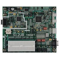
LFEBS12UB Freescale Semiconductor, LFEBS12UB Datasheet - Page 1016

LFEBS12UB
Manufacturer Part Number
LFEBS12UB
Description
KIT STUDENT LEARNING S12 DG128
Manufacturer
Freescale Semiconductor
Specifications of LFEBS12UB
Architecture
8/16-bit
Code Gen Tools Included
Code Warrior
Silicon Manufacturer
Freescale
Core Architecture
S12
Core Sub-architecture
S12
Silicon Core Number
MC9S12
Silicon Family Name
S12D
Kit Contents
HCS12 DG128 Learning Kit
Rohs Compliant
Yes
Lead Free Status / RoHS Status
Lead free / RoHS Compliant
- Current page: 1016 of 1328
- Download datasheet (9Mb)
Chapter 26 384 KByte Flash Module (S12XFTM384K2V1)
(0x7F_FF0F). The Verify Backdoor Access Key command sequence has no effect on the program and
erase protections defined in the Flash protection register, FPROT.
26.5.2
The MCU can be unsecured in special single chip mode by erasing the P-Flash and D-Flash memory by
one of the following methods:
After the CCIF flag sets to indicate that the Erase All Blocks operation has completed, reset the MCU into
special single chip mode. The BDM will execute the Erase Verify All Blocks command write sequence to
verify that the P-Flash and D-Flash memory is erased. If the P-Flash and D-Flash memory are verified as
erased the MCU will be unsecured. All BDM commands will be enabled and the Flash security byte may
be programmed to the unsecure state by the following method:
26.5.3
The availability of Flash module commands depends on the MCU operating mode and security state as
shown in
26.6
On each system reset the Flash module executes a reset sequence which establishes initial values for the
Flash Block Configuration Parameters, the FPROT and DFPROT protection registers, and the FOPT and
FSEC registers. The Flash module reverts to built-in default values that leave the module in a fully
protected and secured state if errors are encountered during execution of the reset sequence. If a double bit
fault is detected during the reset sequence, both MGSTAT bits in the FSTAT register will be set. The
ACCERR bit in the FSTAT register is set if errors are encountered while initializing the EEE buffer ram
during the reset sequence.
CCIF remains clear throughout the reset sequence. The Flash module holds off all CPU access for the
initial portion of the reset sequence. While Flash reads are possible when the hold is removed, writes to
the FCCOBIX, FCCOBHI, and FCCOBLO registers are ignored to prevent command activity while the
Memory Controller remains busy. Completion of the reset sequence is marked by setting CCIF high which
enables writes to the FCCOBIX, FCCOBHI, and FCCOBLO registers to launch any available Flash
command.
If a reset occurs while any Flash command is in progress, that command will be immediately aborted. The
state of the word being programmed or the sector/block being erased is not guaranteed.
1016
•
•
•
Reset the MCU into special single chip mode, delay while the erase test is performed by the BDM,
send BDM commands to disable protection in the P-Flash and D-Flash memory, and execute the
Erase All Blocks command write sequence to erase the P-Flash and D-Flash memory.
Reset the MCU into special expanded wide mode, disable protection in the P-Flash and D-Flash
memory and run code from external memory to execute the Erase All Blocks command write
sequence to erase the P-Flash and D-Flash memory.
Send BDM commands to execute a ‘Program P-Flash’ command sequence to program the Flash
security byte to the unsecured state and reset the MCU.
Table
Initialization
Unsecuring the MCU in Special Single Chip Mode using BDM
Mode and Security Effects on Flash Command Availability
26-30.
MC9S12XE-Family Reference Manual , Rev. 1.23
Freescale Semiconductor
Related parts for LFEBS12UB
Image
Part Number
Description
Manufacturer
Datasheet
Request
R
Part Number:
Description:
Manufacturer:
Freescale Semiconductor, Inc
Datasheet:
Part Number:
Description:
Manufacturer:
Freescale Semiconductor, Inc
Datasheet:
Part Number:
Description:
Manufacturer:
Freescale Semiconductor, Inc
Datasheet:
Part Number:
Description:
Manufacturer:
Freescale Semiconductor, Inc
Datasheet:
Part Number:
Description:
Manufacturer:
Freescale Semiconductor, Inc
Datasheet:
Part Number:
Description:
Manufacturer:
Freescale Semiconductor, Inc
Datasheet:
Part Number:
Description:
Manufacturer:
Freescale Semiconductor, Inc
Datasheet:
Part Number:
Description:
Manufacturer:
Freescale Semiconductor, Inc
Datasheet:
Part Number:
Description:
Manufacturer:
Freescale Semiconductor, Inc
Datasheet:
Part Number:
Description:
Manufacturer:
Freescale Semiconductor, Inc
Datasheet:
Part Number:
Description:
Manufacturer:
Freescale Semiconductor, Inc
Datasheet:
Part Number:
Description:
Manufacturer:
Freescale Semiconductor, Inc
Datasheet:
Part Number:
Description:
Manufacturer:
Freescale Semiconductor, Inc
Datasheet:
Part Number:
Description:
Manufacturer:
Freescale Semiconductor, Inc
Datasheet:
Part Number:
Description:
Manufacturer:
Freescale Semiconductor, Inc
Datasheet:


