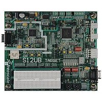
LFEBS12UB Freescale Semiconductor, LFEBS12UB Datasheet - Page 206

LFEBS12UB
Manufacturer Part Number
LFEBS12UB
Description
KIT STUDENT LEARNING S12 DG128
Manufacturer
Freescale Semiconductor
Specifications of LFEBS12UB
Architecture
8/16-bit
Code Gen Tools Included
Code Warrior
Silicon Manufacturer
Freescale
Core Architecture
S12
Core Sub-architecture
S12
Silicon Core Number
MC9S12
Silicon Family Name
S12D
Kit Contents
HCS12 DG128 Learning Kit
Rohs Compliant
Yes
Lead Free Status / RoHS Status
Lead free / RoHS Compliant
- Current page: 206 of 1328
- Download datasheet (9Mb)
Chapter 3 Memory Mapping Control (S12XMMCV4)
The fixed 16K page from 0x4000–0x7FFF (when ROMHM = 0) is the page number 0xFD.
The reset value of 0xFE ensures that there is linear Flash space available between addresses 0x4000 and
0xFFFF out of reset.
The fixed 16K page from 0xC000-0xFFFF is the page number 0xFF.
3.3.2.7
Read: Anytime
Write: Anytime
These eight index bits are used to page 4 KByte blocks into the RAM page window located in the local
(CPU or BDM) memory map from address 0x1000 to address 0x1FFF (see
accessing up to 1022 KByte of RAM (in the Global map) within the 64 KByte Local map. The RAM page
index register is effectively used to construct paged RAM addresses in the Local map
206
Address: 0x0016
Because of an order from the United States International Trade Commission, BGA-packaged product lines and partnumbers
Reset
indicated here currently are not available from Freescale for import or sale in the United States prior to September 2010
W
R
RP7
RAM Page Index Register (RPAGE)
1
7
XGATE write access to this register during an CPU access which makes use
of this register could lead to unexpected results.
Because RAM page 0 has the same global address as the register space, it is
possible to write to registers through the RAM space when RPAGE = 0x00.
0
0
RP6
1
6
Figure 3-13. RAM Page Index Register (RPAGE)
0
MC9S12XE-Family Reference Manual , Rev. 1.23
Figure 3-14. RPAGE Address Mapping
Bit19
Global Address [22:0]
RP5
5
1
Bit18
RPAGE Register [7:0]
CAUTION
RP4
NOTE
1
4
Bit12
Address: CPU Local Address
RP3
1
3
Bit11
or BDM Local Address
Address [11:0]
RP2
2
1
Figure
3-14). This supports
Bit0
Freescale Semiconductor
RP1
format.
0
1
RP0
1
0
Related parts for LFEBS12UB
Image
Part Number
Description
Manufacturer
Datasheet
Request
R
Part Number:
Description:
Manufacturer:
Freescale Semiconductor, Inc
Datasheet:
Part Number:
Description:
Manufacturer:
Freescale Semiconductor, Inc
Datasheet:
Part Number:
Description:
Manufacturer:
Freescale Semiconductor, Inc
Datasheet:
Part Number:
Description:
Manufacturer:
Freescale Semiconductor, Inc
Datasheet:
Part Number:
Description:
Manufacturer:
Freescale Semiconductor, Inc
Datasheet:
Part Number:
Description:
Manufacturer:
Freescale Semiconductor, Inc
Datasheet:
Part Number:
Description:
Manufacturer:
Freescale Semiconductor, Inc
Datasheet:
Part Number:
Description:
Manufacturer:
Freescale Semiconductor, Inc
Datasheet:
Part Number:
Description:
Manufacturer:
Freescale Semiconductor, Inc
Datasheet:
Part Number:
Description:
Manufacturer:
Freescale Semiconductor, Inc
Datasheet:
Part Number:
Description:
Manufacturer:
Freescale Semiconductor, Inc
Datasheet:
Part Number:
Description:
Manufacturer:
Freescale Semiconductor, Inc
Datasheet:
Part Number:
Description:
Manufacturer:
Freescale Semiconductor, Inc
Datasheet:
Part Number:
Description:
Manufacturer:
Freescale Semiconductor, Inc
Datasheet:
Part Number:
Description:
Manufacturer:
Freescale Semiconductor, Inc
Datasheet:


