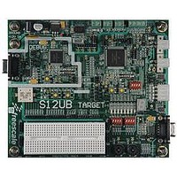
LFEBS12UB Freescale Semiconductor, LFEBS12UB Datasheet - Page 295

LFEBS12UB
Manufacturer Part Number
LFEBS12UB
Description
KIT STUDENT LEARNING S12 DG128
Manufacturer
Freescale Semiconductor
Specifications of LFEBS12UB
Architecture
8/16-bit
Code Gen Tools Included
Code Warrior
Silicon Manufacturer
Freescale
Core Architecture
S12
Core Sub-architecture
S12
Silicon Core Number
MC9S12
Silicon Family Name
S12D
Kit Contents
HCS12 DG128 Learning Kit
Rohs Compliant
Yes
Lead Free Status / RoHS Status
Lead free / RoHS Compliant
- Current page: 295 of 1328
- Download datasheet (9Mb)
7.4.6
The BDM communicates with external devices serially via the BKGD pin. During reset, this pin is a mode
select input which selects between normal and special modes of operation. After reset, this pin becomes
the dedicated serial interface pin for the BDM.
The BDM serial interface is timed using the clock selected by the CLKSW bit in the status register see
Section 7.3.2.1, “BDM Status Register
the following explanation.
The BDM serial interface uses a clocking scheme in which the external host generates a falling edge on
the BKGD pin to indicate the start of each bit time. This falling edge is sent for every bit whether data is
transmitted or received. Data is transferred most significant bit (MSB) first at 16 target clock cycles per
bit. The interface times out if 512 clock cycles occur between falling edges from the host.
The BKGD pin is a pseudo open-drain pin and has an weak on-chip active pull-up that is enabled at all
times. It is assumed that there is an external pull-up and that drivers connected to BKGD do not typically
drive the high level. Since R-C rise time could be unacceptably long, the target system and host provide
brief driven-high (speedup) pulses to drive BKGD to a logic 1. The source of this speedup pulse is the host
for transmit cases and the target for receive cases.
The timing for host-to-target is shown in
Figure
the host and target are operating from separate clocks, it can take the target system up to one full clock
cycle to recognize this edge. The target measures delays from this perceived start of the bit time while the
host measures delays from the point it actually drove BKGD low to start the bit up to one target clock cycle
Freescale Semiconductor
Because of an order from the United States International Trade Commission, BGA-packaged product lines and partnumbers
indicated here currently are not available from Freescale for import or sale in the United States prior to September 2010
Hardware
Hardware
Firmware
Firmware
7-10. All four cases begin when the host drives the BKGD pin low to generate a falling edge. Since
TRACE
Read
Write
Read
Write
GO,
BDM Serial Interface
AT ~16 TC/Bit
Command
Command
Command
Command
Command
8 Bits
DELAY
48-BC
76-BC
Delay
MC9S12XE-Family Reference Manual Rev. 1.23
AT ~16 TC/Bit
Figure 7-7. BDM Command Structure
Address
Address
16 Bits
Data
Command
(BDMSTS)”. This clock will be referred to as the target clock in
Next
Data
Figure 7-8
DELAY
36-BC
and that of target-to-host in
150-BC
Delay
Command
Command
Next
Next
Data
Chapter 7 Background Debug Module (S12XBDMV2)
AT ~16 TC/Bit
16 Bits
Data
BC = Bus Clock Cycles
TC = Target Clock Cycles
150-BC
Delay
Figure 7-9
Command
Command
Next
Next
and
295
Related parts for LFEBS12UB
Image
Part Number
Description
Manufacturer
Datasheet
Request
R
Part Number:
Description:
Manufacturer:
Freescale Semiconductor, Inc
Datasheet:
Part Number:
Description:
Manufacturer:
Freescale Semiconductor, Inc
Datasheet:
Part Number:
Description:
Manufacturer:
Freescale Semiconductor, Inc
Datasheet:
Part Number:
Description:
Manufacturer:
Freescale Semiconductor, Inc
Datasheet:
Part Number:
Description:
Manufacturer:
Freescale Semiconductor, Inc
Datasheet:
Part Number:
Description:
Manufacturer:
Freescale Semiconductor, Inc
Datasheet:
Part Number:
Description:
Manufacturer:
Freescale Semiconductor, Inc
Datasheet:
Part Number:
Description:
Manufacturer:
Freescale Semiconductor, Inc
Datasheet:
Part Number:
Description:
Manufacturer:
Freescale Semiconductor, Inc
Datasheet:
Part Number:
Description:
Manufacturer:
Freescale Semiconductor, Inc
Datasheet:
Part Number:
Description:
Manufacturer:
Freescale Semiconductor, Inc
Datasheet:
Part Number:
Description:
Manufacturer:
Freescale Semiconductor, Inc
Datasheet:
Part Number:
Description:
Manufacturer:
Freescale Semiconductor, Inc
Datasheet:
Part Number:
Description:
Manufacturer:
Freescale Semiconductor, Inc
Datasheet:
Part Number:
Description:
Manufacturer:
Freescale Semiconductor, Inc
Datasheet:


