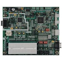
LFEBS12UB Freescale Semiconductor, LFEBS12UB Datasheet - Page 212

LFEBS12UB
Manufacturer Part Number
LFEBS12UB
Description
KIT STUDENT LEARNING S12 DG128
Manufacturer
Freescale Semiconductor
Specifications of LFEBS12UB
Architecture
8/16-bit
Code Gen Tools Included
Code Warrior
Silicon Manufacturer
Freescale
Core Architecture
S12
Core Sub-architecture
S12
Silicon Core Number
MC9S12
Silicon Family Name
S12D
Kit Contents
HCS12 DG128 Learning Kit
Rohs Compliant
Yes
Lead Free Status / RoHS Status
Lead free / RoHS Compliant
- Current page: 212 of 1328
- Download datasheet (9Mb)
Chapter 3 Memory Mapping Control (S12XMMCV4)
Expansion of the BDM Local Address Map
PPAGE, RPAGE, and EPAGE registers are also used for the expansion of the BDM local address to the
global address. These registers can be read and written by the BDM.
The BDM expansion scheme is the same as the CPU expansion scheme.
3.4.2.2
Global Addresses Based on the Global Page
CPU Global Addresses Based on the Global Page
The seven global page index bits allow access to the full 8 Mbyte address map that can be accessed with
23 address bits. This provides an alternative way to access all of the various pages of FLASH, RAM and
EEE as well as additional external memory.
The GPAGE Register is used only when the CPU is executing a global instruction (see
Section 3.3.2.3,
“Global Page Index Register
(GPAGE)). The generated global address is the result of concatenation of the
CPU local address [15:0] with the GPAGE register [22:16] (see
Figure
3-7).
BDM Global Addresses Based on the Global Page
The seven BDMGPR Global Page index bits allow access to the full 8 Mbyte address map that can be
accessed with 23 address bits. This provides an alternative way to access all of the various pages of
FLASH, RAM and EEE as well as additional external memory.
The BDM global page index register (BDMGPR) is used only in the case the CPU is executing a firmware
command which uses a global instruction (like GLDD, GSTD) or by a BDM hardware command (like
WRITE_W, WRITE_BYTE, READ_W, READ_BYTE). See the BDM Block Guide for further details.
The generated global address is a result of concatenation of the BDM local address with the BDMGPR
register [22:16] in the case of a hardware command or concatenation of the CPU local address and the
BDMGPR register [22:16] in the case of a firmware command (see
Figure
3-18).
MC9S12XE-Family Reference Manual , Rev. 1.23
212
Freescale Semiconductor
Because of an order from the United States International Trade Commission, BGA-packaged product lines and partnumbers
indicated here currently are not available from Freescale for import or sale in the United States prior to September 2010
Related parts for LFEBS12UB
Image
Part Number
Description
Manufacturer
Datasheet
Request
R
Part Number:
Description:
Manufacturer:
Freescale Semiconductor, Inc
Datasheet:
Part Number:
Description:
Manufacturer:
Freescale Semiconductor, Inc
Datasheet:
Part Number:
Description:
Manufacturer:
Freescale Semiconductor, Inc
Datasheet:
Part Number:
Description:
Manufacturer:
Freescale Semiconductor, Inc
Datasheet:
Part Number:
Description:
Manufacturer:
Freescale Semiconductor, Inc
Datasheet:
Part Number:
Description:
Manufacturer:
Freescale Semiconductor, Inc
Datasheet:
Part Number:
Description:
Manufacturer:
Freescale Semiconductor, Inc
Datasheet:
Part Number:
Description:
Manufacturer:
Freescale Semiconductor, Inc
Datasheet:
Part Number:
Description:
Manufacturer:
Freescale Semiconductor, Inc
Datasheet:
Part Number:
Description:
Manufacturer:
Freescale Semiconductor, Inc
Datasheet:
Part Number:
Description:
Manufacturer:
Freescale Semiconductor, Inc
Datasheet:
Part Number:
Description:
Manufacturer:
Freescale Semiconductor, Inc
Datasheet:
Part Number:
Description:
Manufacturer:
Freescale Semiconductor, Inc
Datasheet:
Part Number:
Description:
Manufacturer:
Freescale Semiconductor, Inc
Datasheet:
Part Number:
Description:
Manufacturer:
Freescale Semiconductor, Inc
Datasheet:


