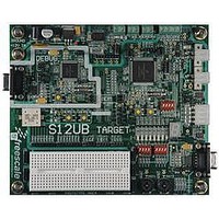
LFEBS12UB Freescale Semiconductor, LFEBS12UB Datasheet - Page 501

LFEBS12UB
Manufacturer Part Number
LFEBS12UB
Description
KIT STUDENT LEARNING S12 DG128
Manufacturer
Freescale Semiconductor
Specifications of LFEBS12UB
Architecture
8/16-bit
Code Gen Tools Included
Code Warrior
Silicon Manufacturer
Freescale
Core Architecture
S12
Core Sub-architecture
S12
Silicon Core Number
MC9S12
Silicon Family Name
S12D
Kit Contents
HCS12 DG128 Learning Kit
Rohs Compliant
Yes
Lead Free Status / RoHS Status
Lead free / RoHS Compliant
- Current page: 501 of 1328
- Download datasheet (9Mb)
Chapter 12
Pierce Oscillator (S12XOSCLCPV2)
12.1
The Pierce oscillator (XOSC) module provides a robust, low-noise and low-power clock source. The
module will be operated from the V
of external components. It is designed for optimal start-up margin with typical crystal oscillators.
12.1.1
The XOSC will contain circuitry to dynamically control current gain in the output amplitude. This ensures
a signal with low harmonic distortion, low power and good noise immunity.
12.1.2
Two modes of operation exist:
The oscillator mode selection is described in the Device Overview section, subsection Oscillator
Configuration.
Freescale Semiconductor
Revision
Because of an order from the United States International Trade Commission, BGA-packaged product lines and partnumbers
Number
V01.05
V02.00
indicated here currently are not available from Freescale for import or sale in the United States prior to September 2010
•
•
•
•
•
•
•
1. Loop controlled Pierce (LCP) oscillator
2. External square wave mode featuring also full swing Pierce (FSP) without internal bias resistor
High noise immunity due to input hysteresis
Low RF emissions with peak-to-peak swing limited dynamically
Transconductance (gm) sized for optimum start-up margin for typical oscillators
Dynamic gain control eliminates the need for external current limiting resistor
Integrated resistor eliminates the need for external bias resistor in loop controlled Pierce mode.
Low power consumption:
— Operates from 1.8 V (nominal) supply
— Amplitude control limits power
Clock monitor
Introduction
Features
Modes of Operation
04 Aug 2006
19 Jul 2006
Revision
Date
Sections
Affected
MC9S12XE-Family Reference Manual , Rev. 1.23
DDPLL
Table 12-1. Revision History
- All xclks info was removed
- Incremented revision to match the design system spec revision
supply rail (1.8 V nominal) and require the minimum number
Description of Changes
501
Related parts for LFEBS12UB
Image
Part Number
Description
Manufacturer
Datasheet
Request
R
Part Number:
Description:
Manufacturer:
Freescale Semiconductor, Inc
Datasheet:
Part Number:
Description:
Manufacturer:
Freescale Semiconductor, Inc
Datasheet:
Part Number:
Description:
Manufacturer:
Freescale Semiconductor, Inc
Datasheet:
Part Number:
Description:
Manufacturer:
Freescale Semiconductor, Inc
Datasheet:
Part Number:
Description:
Manufacturer:
Freescale Semiconductor, Inc
Datasheet:
Part Number:
Description:
Manufacturer:
Freescale Semiconductor, Inc
Datasheet:
Part Number:
Description:
Manufacturer:
Freescale Semiconductor, Inc
Datasheet:
Part Number:
Description:
Manufacturer:
Freescale Semiconductor, Inc
Datasheet:
Part Number:
Description:
Manufacturer:
Freescale Semiconductor, Inc
Datasheet:
Part Number:
Description:
Manufacturer:
Freescale Semiconductor, Inc
Datasheet:
Part Number:
Description:
Manufacturer:
Freescale Semiconductor, Inc
Datasheet:
Part Number:
Description:
Manufacturer:
Freescale Semiconductor, Inc
Datasheet:
Part Number:
Description:
Manufacturer:
Freescale Semiconductor, Inc
Datasheet:
Part Number:
Description:
Manufacturer:
Freescale Semiconductor, Inc
Datasheet:
Part Number:
Description:
Manufacturer:
Freescale Semiconductor, Inc
Datasheet:


