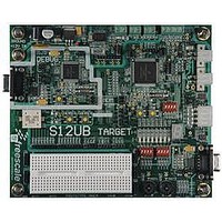
LFEBS12UB Freescale Semiconductor, LFEBS12UB Datasheet - Page 778

LFEBS12UB
Manufacturer Part Number
LFEBS12UB
Description
KIT STUDENT LEARNING S12 DG128
Manufacturer
Freescale Semiconductor
Specifications of LFEBS12UB
Architecture
8/16-bit
Code Gen Tools Included
Code Warrior
Silicon Manufacturer
Freescale
Core Architecture
S12
Core Sub-architecture
S12
Silicon Core Number
MC9S12
Silicon Family Name
S12D
Kit Contents
HCS12 DG128 Learning Kit
Rohs Compliant
Yes
Lead Free Status / RoHS Status
Lead free / RoHS Compliant
- Current page: 778 of 1328
- Download datasheet (9Mb)
Chapter 21 Serial Peripheral Interface (S12SPIV5)
As long as no more than one slave device drives the system slave’s serial data output line, it is possible for
several slaves to receive the same transmission from a master, although the master would not receive return
information from all of the receiving slaves.
If the CPHA bit in SPI control register 1 is clear, odd numbered edges on the SCK input cause the data at
the serial data input pin to be latched. Even numbered edges cause the value previously latched from the
serial data input pin to shift into the LSB or MSB of the SPI shift register, depending on the LSBFE bit.
If the CPHA bit is set, even numbered edges on the SCK input cause the data at the serial data input pin to
be latched. Odd numbered edges cause the value previously latched from the serial data input pin to shift
into the LSB or MSB of the SPI shift register, depending on the LSBFE bit.
When CPHA is set, the first edge is used to get the first data bit onto the serial data output pin. When CPHA
is clear and the SS input is low (slave selected), the first bit of the SPI data is driven out of the serial data
output pin. After the nth
the SPI data register. To indicate transfer is complete, the SPIF flag in the SPI status register is set.
21.4.3
During an SPI transmission, data is transmitted (shifted out serially) and received (shifted in serially)
simultaneously. The serial clock (SCK) synchronizes shifting and sampling of the information on the two
serial data lines. A slave select line allows selection of an individual slave SPI device; slave devices that
are not selected do not interfere with SPI bus activities. Optionally, on a master SPI device, the slave select
line can be used to indicate multiple-master bus contention.
21.4.3.1
Using two bits in the SPI control register 1, software selects one of four combinations of serial clock phase
and polarity.
1. n depends on the selected transfer width, please refer to
778
Because of an order from the United States International Trade Commission, BGA-packaged product lines and partnumbers
indicated here currently are not available from Freescale for import or sale in the United States prior to September 2010
Transmission Formats
Clock Phase and Polarity Controls
A change of the bits CPOL, CPHA, SSOE, LSBFE, MODFEN, SPC0, or
BIDIROE with SPC0 set in slave mode will corrupt a transmission in
progress and must be avoided.
SHIFT REGISTER
GENERATOR
BAUD RATE
MASTER SPI
1
shift, the transfer is considered complete and the received data is transferred into
Figure 21-11. Master/Slave Transfer Block Diagram
MC9S12XE-Family Reference Manual , Rev. 1.23
MISO
MOSI
SCK
SS
NOTE
Section 21.3.2.2, “SPI Control Register 2 (SPICR2)
V
DD
MISO
MOSI
SCK
SS
SHIFT REGISTER
SLAVE SPI
Freescale Semiconductor
Related parts for LFEBS12UB
Image
Part Number
Description
Manufacturer
Datasheet
Request
R
Part Number:
Description:
Manufacturer:
Freescale Semiconductor, Inc
Datasheet:
Part Number:
Description:
Manufacturer:
Freescale Semiconductor, Inc
Datasheet:
Part Number:
Description:
Manufacturer:
Freescale Semiconductor, Inc
Datasheet:
Part Number:
Description:
Manufacturer:
Freescale Semiconductor, Inc
Datasheet:
Part Number:
Description:
Manufacturer:
Freescale Semiconductor, Inc
Datasheet:
Part Number:
Description:
Manufacturer:
Freescale Semiconductor, Inc
Datasheet:
Part Number:
Description:
Manufacturer:
Freescale Semiconductor, Inc
Datasheet:
Part Number:
Description:
Manufacturer:
Freescale Semiconductor, Inc
Datasheet:
Part Number:
Description:
Manufacturer:
Freescale Semiconductor, Inc
Datasheet:
Part Number:
Description:
Manufacturer:
Freescale Semiconductor, Inc
Datasheet:
Part Number:
Description:
Manufacturer:
Freescale Semiconductor, Inc
Datasheet:
Part Number:
Description:
Manufacturer:
Freescale Semiconductor, Inc
Datasheet:
Part Number:
Description:
Manufacturer:
Freescale Semiconductor, Inc
Datasheet:
Part Number:
Description:
Manufacturer:
Freescale Semiconductor, Inc
Datasheet:
Part Number:
Description:
Manufacturer:
Freescale Semiconductor, Inc
Datasheet:


