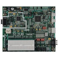
LFEBS12UB Freescale Semiconductor, LFEBS12UB Datasheet - Page 914

LFEBS12UB
Manufacturer Part Number
LFEBS12UB
Description
KIT STUDENT LEARNING S12 DG128
Manufacturer
Freescale Semiconductor
Specifications of LFEBS12UB
Architecture
8/16-bit
Code Gen Tools Included
Code Warrior
Silicon Manufacturer
Freescale
Core Architecture
S12
Core Sub-architecture
S12
Silicon Core Number
MC9S12
Silicon Family Name
S12D
Kit Contents
HCS12 DG128 Learning Kit
Rohs Compliant
Yes
Lead Free Status / RoHS Status
Lead free / RoHS Compliant
- Current page: 914 of 1328
- Download datasheet (9Mb)
Chapter 25 256 KByte Flash Module (S12XFTM256K2V1)
The (unreserved) bits of the FPROT register are writable with the restriction that the size of the protected
region can only be increased (see
During the reset sequence, the FPROT register is loaded with the contents of the P-Flash protection byte
in the Flash configuration field at global address 0x7F_FF0C located in P-Flash memory (see
as indicated by reset condition ‘F’ in
during the reset sequence, the upper sector of the P-Flash memory must be unprotected, then the P-Flash
protection byte must be reprogrammed. If a double bit fault is detected while reading the P-Flash phrase
containing the P-Flash protection byte during the reset sequence, the FPOPEN bit will be cleared and
remaining bits in the FPROT register will be set to leave the P-Flash memory fully protected.
Trying to alter data in any protected area in the P-Flash memory will result in a protection violation error
and the FPVIOL bit will be set in the FSTAT register. The block erase of a P-Flash block is not possible
if any of the P-Flash sectors contained in the same P-Flash block are protected.
914
FPHS[1:0]
FPLS[1:0]
FPOPEN
FPHDIS
FPLDIS
Offset Module Base + 0x0008
RNV[6]
Reset
Field
4–3
1–0
7
6
5
2
W
R
FPOPEN
Flash Protection Operation Enable — The FPOPEN bit determines the protection function for program or
erase operations as shown in
0 When FPOPEN is clear, the FPHDIS and FPLDIS bits define unprotected address ranges as specified by the
1 When FPOPEN is set, the FPHDIS and FPLDIS bits enable protection for the address range specified by the
Reserved Nonvolatile Bit — The RNV bit should remain in the erased state for future enhancements.
Flash Protection Higher Address Range Disable — The FPHDIS bit determines whether there is a
protected/unprotected area in a specific region of the P-Flash memory ending with global address 0x7F_FFFF.
0 Protection/Unprotection enabled
1 Protection/Unprotection disabled
Flash Protection Higher Address Size — The FPHS bits determine the size of the protected/unprotected area
in P-Flash memory as shown
Flash Protection Lower Address Range Disable — The FPLDIS bit determines whether there is a
protected/unprotected area in a specific region of the P-Flash memory beginning with global address
0x7F_8000.
0 Protection/Unprotection enabled
1 Protection/Unprotection disabled
Flash Protection Lower Address Size — The FPLS bits determine the size of the protected/unprotected area
in P-Flash memory as shown in
F
7
corresponding FPHS and FPLS bits
corresponding FPHS and FPLS bits
= Unimplemented or Reserved
RNV6
F
6
Figure 25-13. Flash Protection Register (FPROT)
MC9S12XE-Family Reference Manual , Rev. 1.23
Section 25.3.2.9.1, “P-Flash Protection Restrictions,” and Table
Table 25-19. FPROT Field Descriptions
FPHDIS
Figure
inTable
Table 25-20
F
5
Table
25-21. The FPHS bits can only be written to while the FPHDIS bit is set.
25-22. The FPLS bits can only be written to while the FPLDIS bit is set.
25-13. To change the P-Flash protection that will be loaded
for the P-Flash block.
F
4
FPHS[1:0]
Description
F
3
FPLDIS
F
2
Freescale Semiconductor
F
1
FPLS[1:0]
Table
25-23).
F
0
25-3)
Related parts for LFEBS12UB
Image
Part Number
Description
Manufacturer
Datasheet
Request
R
Part Number:
Description:
Manufacturer:
Freescale Semiconductor, Inc
Datasheet:
Part Number:
Description:
Manufacturer:
Freescale Semiconductor, Inc
Datasheet:
Part Number:
Description:
Manufacturer:
Freescale Semiconductor, Inc
Datasheet:
Part Number:
Description:
Manufacturer:
Freescale Semiconductor, Inc
Datasheet:
Part Number:
Description:
Manufacturer:
Freescale Semiconductor, Inc
Datasheet:
Part Number:
Description:
Manufacturer:
Freescale Semiconductor, Inc
Datasheet:
Part Number:
Description:
Manufacturer:
Freescale Semiconductor, Inc
Datasheet:
Part Number:
Description:
Manufacturer:
Freescale Semiconductor, Inc
Datasheet:
Part Number:
Description:
Manufacturer:
Freescale Semiconductor, Inc
Datasheet:
Part Number:
Description:
Manufacturer:
Freescale Semiconductor, Inc
Datasheet:
Part Number:
Description:
Manufacturer:
Freescale Semiconductor, Inc
Datasheet:
Part Number:
Description:
Manufacturer:
Freescale Semiconductor, Inc
Datasheet:
Part Number:
Description:
Manufacturer:
Freescale Semiconductor, Inc
Datasheet:
Part Number:
Description:
Manufacturer:
Freescale Semiconductor, Inc
Datasheet:
Part Number:
Description:
Manufacturer:
Freescale Semiconductor, Inc
Datasheet:


