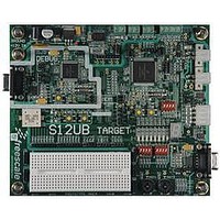
LFEBS12UB Freescale Semiconductor, LFEBS12UB Datasheet - Page 1164

LFEBS12UB
Manufacturer Part Number
LFEBS12UB
Description
KIT STUDENT LEARNING S12 DG128
Manufacturer
Freescale Semiconductor
Specifications of LFEBS12UB
Architecture
8/16-bit
Code Gen Tools Included
Code Warrior
Silicon Manufacturer
Freescale
Core Architecture
S12
Core Sub-architecture
S12
Silicon Core Number
MC9S12
Silicon Family Name
S12D
Kit Contents
HCS12 DG128 Learning Kit
Rohs Compliant
Yes
Lead Free Status / RoHS Status
Lead free / RoHS Compliant
- Current page: 1164 of 1328
- Download datasheet (9Mb)
Chapter 29 1024 KByte Flash Module (S12XFTM1024K5V2)
All possible P-Flash protection scenarios are shown in
loaded from the Flash memory at global address 0x7F_FF0C during the reset sequence, it can be changed
by the user. The P-Flash protection scheme can be used by applications requiring reprogramming in single
chip mode while providing as much protection as possible if reprogramming is not required.
1164
1. For range sizes, refer to
FPOPEN
FPHS[1:0]
FPLS[1:0]
1
1
1
1
0
0
0
0
Table 29-21. P-Flash Protection Higher Address Range
Table 29-22. P-Flash Protection Lower Address Range
00
01
10
11
00
01
10
11
MC9S12XE-Family Reference Manual , Rev. 1.23
FPHDIS
Table 29-20. P-Flash Protection Function
1
1
0
0
1
1
0
0
0x7F_E000–0x7F_FFFF
0x7F_C000–0x7F_FFFF
0x7F_F800–0x7F_FFFF
0x7F_F000–0x7F_FFFF
Global Address Range
0x7F_8000–0x7F_83FF
0x7F_8000–0x7F_87FF
0x7F_8000–0x7F_8FFF
0x7F_8000–0x7F_9FFF
Global Address Range
Table 29-21
FPLDIS
1
0
1
0
1
0
1
0
and
No P-Flash Protection
Protected Low Range
Protected High Range
Protected High and Low Ranges
Full P-Flash Memory Protected
Unprotected Low Range
Unprotected High Range
Unprotected High and Low Ranges
Table
Figure
29-22.
29-14. Although the protection scheme is
Function
Protected Size
Protected Size
16 Kbytes
(1)
2 Kbytes
4 Kbytes
8 Kbytes
2 Kbytes
4 Kbytes
8 Kbytes
1 Kbyte
Freescale Semiconductor
Related parts for LFEBS12UB
Image
Part Number
Description
Manufacturer
Datasheet
Request
R
Part Number:
Description:
Manufacturer:
Freescale Semiconductor, Inc
Datasheet:
Part Number:
Description:
Manufacturer:
Freescale Semiconductor, Inc
Datasheet:
Part Number:
Description:
Manufacturer:
Freescale Semiconductor, Inc
Datasheet:
Part Number:
Description:
Manufacturer:
Freescale Semiconductor, Inc
Datasheet:
Part Number:
Description:
Manufacturer:
Freescale Semiconductor, Inc
Datasheet:
Part Number:
Description:
Manufacturer:
Freescale Semiconductor, Inc
Datasheet:
Part Number:
Description:
Manufacturer:
Freescale Semiconductor, Inc
Datasheet:
Part Number:
Description:
Manufacturer:
Freescale Semiconductor, Inc
Datasheet:
Part Number:
Description:
Manufacturer:
Freescale Semiconductor, Inc
Datasheet:
Part Number:
Description:
Manufacturer:
Freescale Semiconductor, Inc
Datasheet:
Part Number:
Description:
Manufacturer:
Freescale Semiconductor, Inc
Datasheet:
Part Number:
Description:
Manufacturer:
Freescale Semiconductor, Inc
Datasheet:
Part Number:
Description:
Manufacturer:
Freescale Semiconductor, Inc
Datasheet:
Part Number:
Description:
Manufacturer:
Freescale Semiconductor, Inc
Datasheet:
Part Number:
Description:
Manufacturer:
Freescale Semiconductor, Inc
Datasheet:


