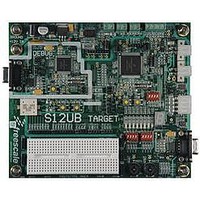
LFEBS12UB Freescale Semiconductor, LFEBS12UB Datasheet - Page 193

LFEBS12UB
Manufacturer Part Number
LFEBS12UB
Description
KIT STUDENT LEARNING S12 DG128
Manufacturer
Freescale Semiconductor
Specifications of LFEBS12UB
Architecture
8/16-bit
Code Gen Tools Included
Code Warrior
Silicon Manufacturer
Freescale
Core Architecture
S12
Core Sub-architecture
S12
Silicon Core Number
MC9S12
Silicon Family Name
S12D
Kit Contents
HCS12 DG128 Learning Kit
Rohs Compliant
Yes
Lead Free Status / RoHS Status
Lead free / RoHS Compliant
- Current page: 193 of 1328
- Download datasheet (9Mb)
3.1.3
The S12X architecture implements a number of memory mapping schemes including
The MMC module performs translation of the different memory mapping schemes to the specific global
(physical) memory implementation.
3.1.4
This subsection lists and briefly describes all operating modes supported by the MMC.
3.1.4.1
3.1.4.2
1. Resources are also called targets.
Freescale Semiconductor
Because of an order from the United States International Trade Commission, BGA-packaged product lines and partnumbers
indicated here currently are not available from Freescale for import or sale in the United States prior to September 2010
•
•
•
•
•
•
•
•
•
•
•
•
•
•
•
•
Simultaneous accesses to different resources
Resolution of target bus access collision
MCU operation mode control
MCU security control
Separate memory map schemes for each master CPU, BDM and XGATE
ROM control bits to enable the on-chip FLASH or ROM selection
Port replacement registers access control
Generation of system reset when CPU accesses an unimplemented address (i.e., an address which
does not belong to any of the on-chip modules) in single-chip modes
a CPU 8 MByte global map, defined using a global page (GPAGE) register and dedicated 23-bit
address load/store instructions.
a BDM 8 MByte global map, defined using a global page (BDMGPR) register and dedicated 23-
bit address load/store instructions.
a (CPU or BDM) 64 KByte local map, defined using specific resource page (RPAGE, EPAGE and
PPAGE) registers and the default instruction set. The 64 KBytes visible at any instant can be
considered as the local map accessed by the 16-bit (CPU or BDM) address.
The XGATE 64 Kbyte local map.
Run mode
MMC is functional during normal run mode.
Wait mode
MMC is functional during wait mode.
Stop mode
MMC is inactive during stop mode.
Single chip modes
In normal and special single chip mode the internal memory is used. External bus is not active.
S12X Memory Mapping
Modes of Operation
Power Saving Modes
Functional Modes
MC9S12XE-Family Reference Manual Rev. 1.23
1
(internal, external, and peripherals) (see
Chapter 3 Memory Mapping Control (S12XMMCV4)
Figure 3-1
193
)
Related parts for LFEBS12UB
Image
Part Number
Description
Manufacturer
Datasheet
Request
R
Part Number:
Description:
Manufacturer:
Freescale Semiconductor, Inc
Datasheet:
Part Number:
Description:
Manufacturer:
Freescale Semiconductor, Inc
Datasheet:
Part Number:
Description:
Manufacturer:
Freescale Semiconductor, Inc
Datasheet:
Part Number:
Description:
Manufacturer:
Freescale Semiconductor, Inc
Datasheet:
Part Number:
Description:
Manufacturer:
Freescale Semiconductor, Inc
Datasheet:
Part Number:
Description:
Manufacturer:
Freescale Semiconductor, Inc
Datasheet:
Part Number:
Description:
Manufacturer:
Freescale Semiconductor, Inc
Datasheet:
Part Number:
Description:
Manufacturer:
Freescale Semiconductor, Inc
Datasheet:
Part Number:
Description:
Manufacturer:
Freescale Semiconductor, Inc
Datasheet:
Part Number:
Description:
Manufacturer:
Freescale Semiconductor, Inc
Datasheet:
Part Number:
Description:
Manufacturer:
Freescale Semiconductor, Inc
Datasheet:
Part Number:
Description:
Manufacturer:
Freescale Semiconductor, Inc
Datasheet:
Part Number:
Description:
Manufacturer:
Freescale Semiconductor, Inc
Datasheet:
Part Number:
Description:
Manufacturer:
Freescale Semiconductor, Inc
Datasheet:
Part Number:
Description:
Manufacturer:
Freescale Semiconductor, Inc
Datasheet:


