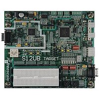
LFEBS12UB Freescale Semiconductor, LFEBS12UB Datasheet - Page 862

LFEBS12UB
Manufacturer Part Number
LFEBS12UB
Description
KIT STUDENT LEARNING S12 DG128
Manufacturer
Freescale Semiconductor
Specifications of LFEBS12UB
Architecture
8/16-bit
Code Gen Tools Included
Code Warrior
Silicon Manufacturer
Freescale
Core Architecture
S12
Core Sub-architecture
S12
Silicon Core Number
MC9S12
Silicon Family Name
S12D
Kit Contents
HCS12 DG128 Learning Kit
Rohs Compliant
Yes
Lead Free Status / RoHS Status
Lead free / RoHS Compliant
- Current page: 862 of 1328
- Download datasheet (9Mb)
Chapter 24 128 KByte Flash Module (S12XFTM128K2V1)
The P-Flash word addressed by ECCRIX = 001 contains the lower 16 bits of the global address. The
following four words addressed by ECCRIX = 010 to 101 contain the 64-bit wide data phrase. The four
data words and the parity byte are the uncorrected data read from the P-Flash block.
The D-Flash word addressed by ECCRIX = 001 contains the lower 16 bits of the global address. The
uncorrected 16-bit data word is addressed by ECCRIX = 010.
24.3.2.14 Flash Option Register (FOPT)
The FOPT register is the Flash option register.
All bits in the FOPT register are readable but are not writable.
During the reset sequence, the FOPT register is loaded from the Flash nonvolatile byte in the Flash
configuration field at global address 0x7F_FF0E located in P-Flash memory (see
by reset condition F in
containing the Flash nonvolatile byte during the reset sequence, all bits in the FOPT register will be set.
24.3.2.15 Flash Reserved0 Register (FRSV0)
This Flash register is reserved for factory testing.
862
GADDR[22:16]
NV[7:0]
Offset Module Base + 0x0010
Reset
PAR[7:0]
XBUS01
Field
7–0
Field
15:8
6–0
W
7
R
Nonvolatile Bits — The NV[7:0] bits are available as nonvolatile bits. Refer to the device user guide for proper
use of the NV bits.
F
7
ECC Parity Bits — Contains the 8 parity bits from the 72 bit wide P-Flash data word or the 6 parity bits,
allocated to PAR[5:0], from the 22 bit wide D-Flash word with PAR[7:6]=00.
Bus Source Identifier — The XBUS01 bit determines whether the ECC error was caused by a read access
from the CPU or XGATE.
0 ECC Error happened on the CPU access
1 ECC Error happened on the XGATE access
Global Address — The GADDR[22:16] field contains the upper seven bits of the global address having
caused the error.
= Unimplemented or Reserved
Figure
F
6
Table 24-28. FECCR Index=000 Bit Descriptions
24-22. If a double bit fault is detected while reading the P-Flash phrase
Figure 24-22. Flash Option Register (FOPT)
MC9S12XE-Family Reference Manual , Rev. 1.23
Table 24-29. FOPT Field Descriptions
F
5
F
4
Description
NV[7:0]
Description
F
3
F
2
Table
Freescale Semiconductor
F
1
24-3) as indicated
F
0
Related parts for LFEBS12UB
Image
Part Number
Description
Manufacturer
Datasheet
Request
R
Part Number:
Description:
Manufacturer:
Freescale Semiconductor, Inc
Datasheet:
Part Number:
Description:
Manufacturer:
Freescale Semiconductor, Inc
Datasheet:
Part Number:
Description:
Manufacturer:
Freescale Semiconductor, Inc
Datasheet:
Part Number:
Description:
Manufacturer:
Freescale Semiconductor, Inc
Datasheet:
Part Number:
Description:
Manufacturer:
Freescale Semiconductor, Inc
Datasheet:
Part Number:
Description:
Manufacturer:
Freescale Semiconductor, Inc
Datasheet:
Part Number:
Description:
Manufacturer:
Freescale Semiconductor, Inc
Datasheet:
Part Number:
Description:
Manufacturer:
Freescale Semiconductor, Inc
Datasheet:
Part Number:
Description:
Manufacturer:
Freescale Semiconductor, Inc
Datasheet:
Part Number:
Description:
Manufacturer:
Freescale Semiconductor, Inc
Datasheet:
Part Number:
Description:
Manufacturer:
Freescale Semiconductor, Inc
Datasheet:
Part Number:
Description:
Manufacturer:
Freescale Semiconductor, Inc
Datasheet:
Part Number:
Description:
Manufacturer:
Freescale Semiconductor, Inc
Datasheet:
Part Number:
Description:
Manufacturer:
Freescale Semiconductor, Inc
Datasheet:
Part Number:
Description:
Manufacturer:
Freescale Semiconductor, Inc
Datasheet:


