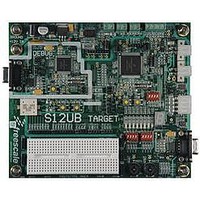
LFEBS12UB Freescale Semiconductor, LFEBS12UB Datasheet - Page 238

LFEBS12UB
Manufacturer Part Number
LFEBS12UB
Description
KIT STUDENT LEARNING S12 DG128
Manufacturer
Freescale Semiconductor
Specifications of LFEBS12UB
Architecture
8/16-bit
Code Gen Tools Included
Code Warrior
Silicon Manufacturer
Freescale
Core Architecture
S12
Core Sub-architecture
S12
Silicon Core Number
MC9S12
Silicon Family Name
S12D
Kit Contents
HCS12 DG128 Learning Kit
Rohs Compliant
Yes
Lead Free Status / RoHS Status
Lead free / RoHS Compliant
- Current page: 238 of 1328
- Download datasheet (9Mb)
Chapter 4 Memory Protection Unit (S12XMPUV1)
4.3.1.6
1. initialized as set for descriptor 0 only, cleared for all others
2. initialized as set for descriptor 0 only, if MSTR3 is implemented on the device
Read: Anytime
Write: Anytime
A descriptor can be configured as valid for more than one bus-master at the same time by setting multiple
Master select bits to one. Setting all Master select bits of a descriptor to zero disables the descriptor.
4.3.1.7
Read: Anytime
Write: Anytime
238
Address: Module Base + 0x0006
Address: Module Base + 0x0007
LOW_ADDR[
Because of an order from the United States International Trade Commission, BGA-packaged product lines and partnumbers
Reset
Reset
MSTR0
MSTR1
MSTR2
MSTR3
indicated here currently are not available from Freescale for import or sale in the United States prior to September 2010
22:19]
Field
3–0
7
6
5
4
W
W
R
R
MSTR0
1
MPU Descriptor Register 0 (MPUDESC0)
MPU Descriptor Register 1 (MPUDESC1)
Master 0 select bit — If this bit is set the descriptor is valid for bus master 0 (CPU in supervisor state).
Master 1 select bit — If this bit is set the descriptor is valid for bus master 1 (CPU in user state).
Master 2 select bit — If this bit is set the descriptor is valid for bus master 2 (XGATE).
Master 3 select bit — If this bit is set the descriptor is valid for bus master 3.
Memory range lower boundary address bits — The LOW_ADDR[22:19] bits represent bits [22:19] of the
global memory address that is used as the lower boundary for the described memory range.
0
7
(1)
7
MSTR1
1
0
6
6
1
Figure 4-8. MPU Descriptor Register 0 (MPUDESC0)
Figure 4-9. MPU Descriptor Register 1 (MPUDESC1)
MC9S12XE-Family Reference Manual , Rev. 1.23
Table 4-8. MPUDESC0 Field Descriptions
MSTR2
1
5
5
0
1
MSTR3
LOW_ADDR[18:11]
1
0
4
(2)
4
Description
0
0
3
3
LOW_ADDR[22:19]
2
0
2
0
Freescale Semiconductor
0
0
1
1
0
0
0
0
Related parts for LFEBS12UB
Image
Part Number
Description
Manufacturer
Datasheet
Request
R
Part Number:
Description:
Manufacturer:
Freescale Semiconductor, Inc
Datasheet:
Part Number:
Description:
Manufacturer:
Freescale Semiconductor, Inc
Datasheet:
Part Number:
Description:
Manufacturer:
Freescale Semiconductor, Inc
Datasheet:
Part Number:
Description:
Manufacturer:
Freescale Semiconductor, Inc
Datasheet:
Part Number:
Description:
Manufacturer:
Freescale Semiconductor, Inc
Datasheet:
Part Number:
Description:
Manufacturer:
Freescale Semiconductor, Inc
Datasheet:
Part Number:
Description:
Manufacturer:
Freescale Semiconductor, Inc
Datasheet:
Part Number:
Description:
Manufacturer:
Freescale Semiconductor, Inc
Datasheet:
Part Number:
Description:
Manufacturer:
Freescale Semiconductor, Inc
Datasheet:
Part Number:
Description:
Manufacturer:
Freescale Semiconductor, Inc
Datasheet:
Part Number:
Description:
Manufacturer:
Freescale Semiconductor, Inc
Datasheet:
Part Number:
Description:
Manufacturer:
Freescale Semiconductor, Inc
Datasheet:
Part Number:
Description:
Manufacturer:
Freescale Semiconductor, Inc
Datasheet:
Part Number:
Description:
Manufacturer:
Freescale Semiconductor, Inc
Datasheet:
Part Number:
Description:
Manufacturer:
Freescale Semiconductor, Inc
Datasheet:


