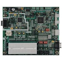
LFEBS12UB Freescale Semiconductor, LFEBS12UB Datasheet - Page 242

LFEBS12UB
Manufacturer Part Number
LFEBS12UB
Description
KIT STUDENT LEARNING S12 DG128
Manufacturer
Freescale Semiconductor
Specifications of LFEBS12UB
Architecture
8/16-bit
Code Gen Tools Included
Code Warrior
Silicon Manufacturer
Freescale
Core Architecture
S12
Core Sub-architecture
S12
Silicon Core Number
MC9S12
Silicon Family Name
S12D
Kit Contents
HCS12 DG128 Learning Kit
Rohs Compliant
Yes
Lead Free Status / RoHS Status
Lead free / RoHS Compliant
- Current page: 242 of 1328
- Download datasheet (9Mb)
Chapter 4 Memory Protection Unit (S12XMPUV1)
4.4.1.1
If the memory ranges of two protection descriptors defined for the same bus-master overlap, the access
restrictions for the overlapped memory range are accumulated. For example:
4.4.1.2
As mentioned in the bit description of the Access Error Flag (AEF) in the MPUFLG register
there is an additional memory range implicitly defined only while the AEF bit is set: The CPU in
supervisor state can read from and write to the peripheral register space even if there is no memory
protection descriptor explicitly allowing this. This is to prevent the case that the CPU cannot clear the AEF
bit if the registers are write protected for the CPU in supervisor state.
The register address space containing the PAGE registers (EPAGE, RPAGE, GPAGE, PPAGE) at 0x0010−
0x0017 gets special treatment. It is defined like this:
4.4.1.3
Some bus-masters (CPU, XGATE) do a pre-fetch of program-code past the current instruction. The
S12XCPU pre-fetches two words past the current instruction, the XGATE pre-fetches one word, even if
the pre-fetched code is not executed. The MPU module has no way of knowing this at the time when the
pre-fetch cycles occur. Therefore this will result in an access violation if the op-code pre-fetch accesses a
memory range marked as “No-Execute” (NEX=1). This must be taken into account when defining memory
242
Because of an order from the United States International Trade Commission, BGA-packaged product lines and partnumbers
indicated here currently are not available from Freescale for import or sale in the United States prior to September 2010
•
•
•
•
•
a memory protection descriptor defines memory range 0x40_0000−0x41_FFFF as WP=1, NEX=0
(read and execute)
another descriptor defines memory range 0x41_0000−0x43_FFFF as WP=0, NEX=1 (read and
write)
the resulting access rights for the overlapping range 0x41_0000−0x41_FFFF are WP=1, NEX=1
(read only)
The S12X CPU can always read and write these registers, regardless of the configuration in the
descriptors.
XGATE or Master3 (if available) are never allowed to read or write these registers, even if the
descriptor configuration allows accesses for other masters than the S12X CPU.
Overlapping Descriptors
Implicitly defined memory descriptors
Op-code pre-fetch cycles and the NEX bit
Configuring the lower boundary address of a descriptor to be higher than the
upper boundary address of a descriptor causes this descriptor to be ignored
by the comparator block. This effectively disables the descriptor.
Avoid changing descriptors while they are in active use to validate accesses
from bus-masters. This can be done by temporarily disabling the affected
master during the update (XGATE, Master 3, switch S12X CPU states).
Otherwise accesses from bus-masters affected by a descriptor which is
updated concurrently could yield undefined results.
MC9S12XE-Family Reference Manual , Rev. 1.23
NOTE
NOTE
Freescale Semiconductor
(Table
4-3),
Related parts for LFEBS12UB
Image
Part Number
Description
Manufacturer
Datasheet
Request
R
Part Number:
Description:
Manufacturer:
Freescale Semiconductor, Inc
Datasheet:
Part Number:
Description:
Manufacturer:
Freescale Semiconductor, Inc
Datasheet:
Part Number:
Description:
Manufacturer:
Freescale Semiconductor, Inc
Datasheet:
Part Number:
Description:
Manufacturer:
Freescale Semiconductor, Inc
Datasheet:
Part Number:
Description:
Manufacturer:
Freescale Semiconductor, Inc
Datasheet:
Part Number:
Description:
Manufacturer:
Freescale Semiconductor, Inc
Datasheet:
Part Number:
Description:
Manufacturer:
Freescale Semiconductor, Inc
Datasheet:
Part Number:
Description:
Manufacturer:
Freescale Semiconductor, Inc
Datasheet:
Part Number:
Description:
Manufacturer:
Freescale Semiconductor, Inc
Datasheet:
Part Number:
Description:
Manufacturer:
Freescale Semiconductor, Inc
Datasheet:
Part Number:
Description:
Manufacturer:
Freescale Semiconductor, Inc
Datasheet:
Part Number:
Description:
Manufacturer:
Freescale Semiconductor, Inc
Datasheet:
Part Number:
Description:
Manufacturer:
Freescale Semiconductor, Inc
Datasheet:
Part Number:
Description:
Manufacturer:
Freescale Semiconductor, Inc
Datasheet:
Part Number:
Description:
Manufacturer:
Freescale Semiconductor, Inc
Datasheet:


