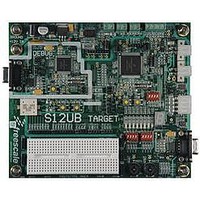
LFEBS12UB Freescale Semiconductor, LFEBS12UB Datasheet - Page 118

LFEBS12UB
Manufacturer Part Number
LFEBS12UB
Description
KIT STUDENT LEARNING S12 DG128
Manufacturer
Freescale Semiconductor
Specifications of LFEBS12UB
Architecture
8/16-bit
Code Gen Tools Included
Code Warrior
Silicon Manufacturer
Freescale
Core Architecture
S12
Core Sub-architecture
S12
Silicon Core Number
MC9S12
Silicon Family Name
S12D
Kit Contents
HCS12 DG128 Learning Kit
Rohs Compliant
Yes
Lead Free Status / RoHS Status
Lead free / RoHS Compliant
- Current page: 118 of 1328
- Download datasheet (9Mb)
1. Read: Anytime. In emulation modes, read operations will return the data from the external bus, in all other modes the data source
1. Read:Anytime in single-chip modes.
Chapter 2 Port Integration Module (S12XEPIMV1)
2.3.12
2.3.13
118
Address 0x0009 (PRR)
Address 0x000C (PRR)
is depending on the data direction value.
Write: Anytime. In emulation modes, write operations will also be directed to the external bus.
Write:Anytime, except BKPUE which is writable in Special Test Mode only.
DDRE
Field
Reset
Reset
7-2
1-0
W
W
R
R
Port E Data Direction—
This register controls the data direction of pins 7 through 2.
The external bus function controls the data direction for the associated pins. In this case the data direction bits will
not change.
When operating a pin as a general purpose I/O, the associated data direction bit determines whether it is an input
or output.
1 Associated pin is configured as output.
0 Associated pin is configured as high-impedance input.
Reserved—
Port E bit 1 (associated with IRQ) and bit 0 (associated with XIRQ) cannot be configured as outputs. Port E, bits 1
and 0, can be read regardless of whether the alternate interrupt function is enabled.
DDRE7
PUPKE
Port E Data Direction Register (DDRE)
S12X_EBI ports, BKGD pin Pull-up Control Register (PUCR)
0
1
7
7
Figure 2-11. S12X_EBI ports, BKGD pin Pull-up Control Register (PUCR)
= Unimplemented or Reserved
= Unimplemented or Reserved
DDRE6
BKPUE
0
1
6
6
Figure 2-10. Port E Data Direction Register (DDRE)
Table 2-13. DDRE Register Field Descriptions
MC9S12XE-Family Reference Manual , Rev. 1.23
DDRE5
0
0
0
5
5
DDRE4
PUPEE
0
1
4
4
Description
DDRE3
PUPDE
3
0
3
0
DDRE2
PUPCE
0
0
2
2
Access: User read/write
Access: User read/write
Freescale Semiconductor
PUPBE
0
0
0
1
1
PUPAE
0
0
0
0
0
(1)
(1)
Related parts for LFEBS12UB
Image
Part Number
Description
Manufacturer
Datasheet
Request
R
Part Number:
Description:
Manufacturer:
Freescale Semiconductor, Inc
Datasheet:
Part Number:
Description:
Manufacturer:
Freescale Semiconductor, Inc
Datasheet:
Part Number:
Description:
Manufacturer:
Freescale Semiconductor, Inc
Datasheet:
Part Number:
Description:
Manufacturer:
Freescale Semiconductor, Inc
Datasheet:
Part Number:
Description:
Manufacturer:
Freescale Semiconductor, Inc
Datasheet:
Part Number:
Description:
Manufacturer:
Freescale Semiconductor, Inc
Datasheet:
Part Number:
Description:
Manufacturer:
Freescale Semiconductor, Inc
Datasheet:
Part Number:
Description:
Manufacturer:
Freescale Semiconductor, Inc
Datasheet:
Part Number:
Description:
Manufacturer:
Freescale Semiconductor, Inc
Datasheet:
Part Number:
Description:
Manufacturer:
Freescale Semiconductor, Inc
Datasheet:
Part Number:
Description:
Manufacturer:
Freescale Semiconductor, Inc
Datasheet:
Part Number:
Description:
Manufacturer:
Freescale Semiconductor, Inc
Datasheet:
Part Number:
Description:
Manufacturer:
Freescale Semiconductor, Inc
Datasheet:
Part Number:
Description:
Manufacturer:
Freescale Semiconductor, Inc
Datasheet:
Part Number:
Description:
Manufacturer:
Freescale Semiconductor, Inc
Datasheet:


