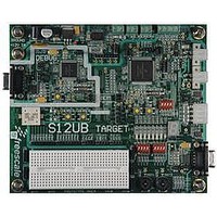
LFEBS12UB Freescale Semiconductor, LFEBS12UB Datasheet - Page 797

LFEBS12UB
Manufacturer Part Number
LFEBS12UB
Description
KIT STUDENT LEARNING S12 DG128
Manufacturer
Freescale Semiconductor
Specifications of LFEBS12UB
Architecture
8/16-bit
Code Gen Tools Included
Code Warrior
Silicon Manufacturer
Freescale
Core Architecture
S12
Core Sub-architecture
S12
Silicon Core Number
MC9S12
Silicon Family Name
S12D
Kit Contents
HCS12 DG128 Learning Kit
Rohs Compliant
Yes
Lead Free Status / RoHS Status
Lead free / RoHS Compliant
- Current page: 797 of 1328
- Download datasheet (9Mb)
Read: Anytime but will always return 0x0000 (1 state is transient)
Write: Anytime
22.3.2.3
Read: Anytime
Write: Anytime
Freescale Semiconductor
Module Base + 0x0002
OC7M[7:0]
Because of an order from the United States International Trade Commission, BGA-packaged product lines and partnumbers
FOC[7:0]
Reset
indicated here currently are not available from Freescale for import or sale in the United States prior to September 2010
Field
Field
7:0
7:0
W
R
OC7M7
Force Output Compare Action for Channel 7:0 — A write to this register with the corresponding data bit(s) set
causes the action which is programmed for output compare “x” to occur immediately. The action taken is the
same as if a successful comparison had just taken place with the TCx register except the interrupt flag does not
get set.
Note: A channel 7 event, which can be a counter overflow when TTOV[7] is set or a successful output compare
Output Compare 7 Mask — A channel 7 event, which can be a counter overflow when TTOV[7] is set or a
successful output compare on channel 7, overrides any channel 6:0 compares. For each OC7M bit that is set,
the output compare action reflects the corresponding OC7D bit.
0 The corresponding OC7Dx bit in the output compare 7 data register will not be transferred to the timer port on
1 The corresponding OC7Dx bit in the output compare 7 data register will be transferred to the timer port on a
Note: The corresponding channel must also be setup for output compare (IOSx = 1 and OCPDx = 0) for data to
Output Compare 7 Mask Register (OC7M)
0
7
a channel 7 event, even if the corresponding pin is setup for output compare.
channel 7 event.
on channel 7, overrides any channel 6:0 compares. If forced output compare on any channel occurs at the
same time as the successful output compare then forced output compare action will take precedence and
interrupt flag won’t get set.
be transferred from the output compare 7 data register to the timer port.
OC7M6
Figure 22-8. Output Compare 7 Mask Register (OC7M)
0
6
MC9S12XE-Family Reference Manual Rev. 1.23
Table 22-3. CFORC Field Descriptions
Table 22-4. OC7M Field Descriptions
OC7M5
5
0
OC7M4
0
4
Description
Description
Chapter 22 Timer Module (TIM16B8CV2) Block Description
OC7M3
0
3
OC7M2
2
0
OC7M1
0
1
OC7M0
0
0
797
Related parts for LFEBS12UB
Image
Part Number
Description
Manufacturer
Datasheet
Request
R
Part Number:
Description:
Manufacturer:
Freescale Semiconductor, Inc
Datasheet:
Part Number:
Description:
Manufacturer:
Freescale Semiconductor, Inc
Datasheet:
Part Number:
Description:
Manufacturer:
Freescale Semiconductor, Inc
Datasheet:
Part Number:
Description:
Manufacturer:
Freescale Semiconductor, Inc
Datasheet:
Part Number:
Description:
Manufacturer:
Freescale Semiconductor, Inc
Datasheet:
Part Number:
Description:
Manufacturer:
Freescale Semiconductor, Inc
Datasheet:
Part Number:
Description:
Manufacturer:
Freescale Semiconductor, Inc
Datasheet:
Part Number:
Description:
Manufacturer:
Freescale Semiconductor, Inc
Datasheet:
Part Number:
Description:
Manufacturer:
Freescale Semiconductor, Inc
Datasheet:
Part Number:
Description:
Manufacturer:
Freescale Semiconductor, Inc
Datasheet:
Part Number:
Description:
Manufacturer:
Freescale Semiconductor, Inc
Datasheet:
Part Number:
Description:
Manufacturer:
Freescale Semiconductor, Inc
Datasheet:
Part Number:
Description:
Manufacturer:
Freescale Semiconductor, Inc
Datasheet:
Part Number:
Description:
Manufacturer:
Freescale Semiconductor, Inc
Datasheet:
Part Number:
Description:
Manufacturer:
Freescale Semiconductor, Inc
Datasheet:


