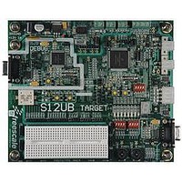
LFEBS12UB Freescale Semiconductor, LFEBS12UB Datasheet - Page 598

LFEBS12UB
Manufacturer Part Number
LFEBS12UB
Description
KIT STUDENT LEARNING S12 DG128
Manufacturer
Freescale Semiconductor
Specifications of LFEBS12UB
Architecture
8/16-bit
Code Gen Tools Included
Code Warrior
Silicon Manufacturer
Freescale
Core Architecture
S12
Core Sub-architecture
S12
Silicon Core Number
MC9S12
Silicon Family Name
S12D
Kit Contents
HCS12 DG128 Learning Kit
Rohs Compliant
Yes
Lead Free Status / RoHS Status
Lead free / RoHS Compliant
- Current page: 598 of 1328
- Download datasheet (9Mb)
Chapter 15 Inter-Integrated Circuit (IICV3) Block Description
15.4.1.5
As shown in
a STOP signal to terminate the communication. This is used by the master to communicate with another
slave or with the same slave in different mode (transmit/receive mode) without releasing the bus.
15.4.1.6
The Inter-IC bus is a true multi-master bus that allows more than one master to be connected on it. If two
or more masters try to control the bus at the same time, a clock synchronization procedure determines the
bus clock, for which the low period is equal to the longest clock low period and the high is equal to the
shortest one among the masters. The relative priority of the contending masters is determined by a data
arbitration procedure, a bus master loses arbitration if it transmits logic 1 while another master transmits
logic 0. The losing masters immediately switch over to slave receive mode and stop driving SDA output.
In this case the transition from master to slave mode does not generate a STOP condition. Meanwhile, a
status bit is set by hardware to indicate loss of arbitration.
15.4.1.7
Because wire-AND logic is performed on SCL line, a high-to-low transition on SCL line affects all the
devices connected on the bus. The devices start counting their low period and as soon as a device's clock
has gone low, it holds the SCL line low until the clock high state is reached.However, the change of low to
high in this device clock may not change the state of the SCL line if another device clock is within its low
period. Therefore, synchronized clock SCL is held low by the device with the longest low period. Devices
with shorter low periods enter a high wait state during this time (see
concerned have counted off their low period, the synchronized clock SCL line is released and pulled high.
There is then no difference between the device clocks and the state of the SCL line and all the devices start
counting their high periods.The first device to complete its high period pulls the SCL line low again.
598
Because of an order from the United States International Trade Commission, BGA-packaged product lines and partnumbers
SCL1
SCL2
indicated here currently are not available from Freescale for import or sale in the United States prior to September 2010
SCL
Figure
Repeated START Signal
Arbitration Procedure
Clock Synchronization
Internal Counter Reset
15-10, a repeated START signal is a START signal generated without first generating
Figure 15-12. IIC-Bus Clock Synchronization
MC9S12XE-Family Reference Manual , Rev. 1.23
WAIT
Start Counting High Period
Figure
15-11). When all devices
Freescale Semiconductor
Related parts for LFEBS12UB
Image
Part Number
Description
Manufacturer
Datasheet
Request
R
Part Number:
Description:
Manufacturer:
Freescale Semiconductor, Inc
Datasheet:
Part Number:
Description:
Manufacturer:
Freescale Semiconductor, Inc
Datasheet:
Part Number:
Description:
Manufacturer:
Freescale Semiconductor, Inc
Datasheet:
Part Number:
Description:
Manufacturer:
Freescale Semiconductor, Inc
Datasheet:
Part Number:
Description:
Manufacturer:
Freescale Semiconductor, Inc
Datasheet:
Part Number:
Description:
Manufacturer:
Freescale Semiconductor, Inc
Datasheet:
Part Number:
Description:
Manufacturer:
Freescale Semiconductor, Inc
Datasheet:
Part Number:
Description:
Manufacturer:
Freescale Semiconductor, Inc
Datasheet:
Part Number:
Description:
Manufacturer:
Freescale Semiconductor, Inc
Datasheet:
Part Number:
Description:
Manufacturer:
Freescale Semiconductor, Inc
Datasheet:
Part Number:
Description:
Manufacturer:
Freescale Semiconductor, Inc
Datasheet:
Part Number:
Description:
Manufacturer:
Freescale Semiconductor, Inc
Datasheet:
Part Number:
Description:
Manufacturer:
Freescale Semiconductor, Inc
Datasheet:
Part Number:
Description:
Manufacturer:
Freescale Semiconductor, Inc
Datasheet:
Part Number:
Description:
Manufacturer:
Freescale Semiconductor, Inc
Datasheet:


