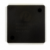
PI7C8152BMAE Pericom Semiconductor, PI7C8152BMAE Datasheet - Page 19

PI7C8152BMAE
Manufacturer Part Number
PI7C8152BMAE
Description
IC PCI-PCI BRIDGE 2PORT 160-MQFP
Manufacturer
Pericom Semiconductor
Datasheet
1.PI7C8152AMAE.pdf
(90 pages)
Specifications of PI7C8152BMAE
Applications
*
Interface
*
Voltage - Supply
*
Package / Case
160-MQFP, 160-PQFP
Mounting Type
Surface Mount
Maximum Operating Temperature
+ 85 C
Minimum Operating Temperature
0 C
Mounting Style
SMD/SMT
Operating Supply Voltage
3 V to 3.6 V
Supply Current (max)
246 mA
Lead Free Status / RoHS Status
Lead free / RoHS Compliant
Available stocks
Company
Part Number
Manufacturer
Quantity
Price
Company:
Part Number:
PI7C8152BMAE
Manufacturer:
PERICOM
Quantity:
748
Part Number:
PI7C8152BMAE
Manufacturer:
PERICOM
Quantity:
20 000
3.4
3.5
3.6
Table 3-2 WRITE TRANSACTION FORWARDING
DEVICE SELECT (DEVSEL_L) GENERATION
PI7C8152x always performs positive address decoding (medium decode) when accepting
transactions on either the primary or secondary buses. PI7C8152x never does subtractive
decode.
DATA PHASE
The address phase of a PCI transaction is followed by one or more data phases.
A data phase is completed when IRDY_L and either TRDY_L or STOP_L are asserted.
A transfer of data occurs only when both IRDY_L and TRDY_L are asserted during the
same PCI clock cycle. The last data phase of a transaction is indicated when FRAME_L is
de-asserted and both TRDY_L and IRDY_L are asserted, or when IRDY_L and STOP_L
are asserted. See Section 3.9 for further discussion of transaction termination.
Depending on the command type, PI7C8152x can support multiple data phase
PCI transactions. For detailed descriptions of how PI7C8152x imposes disconnect
boundaries, see Section 3.6.4 for write address boundaries and Section 3.7.3 read address
boundaries.
WRITE TRANSACTIONS
Write transactions are treated as either posted write or delayed write transactions. Table
3-2 shows the method of forwarding used for each type of write operation.
phase consists of the specific memory transaction command code on the CBE_L[3:0]
lines, and the high 32 address bits on the AD[31:0] lines. In this way, 64-bit addressing
can be supported on 32-bit PCI buses.
The PCI-to-PCI Bridge Architecture Specification supports the use of dual address
transactions in the prefetchable memory range only. See Section 4.3.2 for a discussion of
prefetchable address space. The PI7C8152x supports dual address transactions in both the
upstream and the downstream direction. The PI7C8152x supports a programmable 64-bit
address range in prefetchable memory for downstream forwarding of dual address
transactions. Dual address transactions falling outside the prefetchable address range are
forwarded upstream. Prefetching and posting are performed in a manner consistent with
the guidelines given in this specification for each type of memory transaction in
prefetchable memory space.
Type of Transaction
Memory Write
Memory Write and Invalidate
Memory Write to VGA memory
I/O Write
Type 1 Configuration Write
Page 19 of 90
Type of Forwarding
Posted (except VGA memory)
Posted
Delayed
Delayed
Delayed
2-PORT PCI-TO-PCI BRIDGE
October 16, 2003 – Revision 1.11
ADVANCE INFORMATION
PI7C8152A & PI7C8152B


