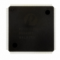
PI7C8152BMAE Pericom Semiconductor, PI7C8152BMAE Datasheet - Page 85

PI7C8152BMAE
Manufacturer Part Number
PI7C8152BMAE
Description
IC PCI-PCI BRIDGE 2PORT 160-MQFP
Manufacturer
Pericom Semiconductor
Datasheet
1.PI7C8152AMAE.pdf
(90 pages)
Specifications of PI7C8152BMAE
Applications
*
Interface
*
Voltage - Supply
*
Package / Case
160-MQFP, 160-PQFP
Mounting Type
Surface Mount
Maximum Operating Temperature
+ 85 C
Minimum Operating Temperature
0 C
Mounting Style
SMD/SMT
Operating Supply Voltage
3 V to 3.6 V
Supply Current (max)
246 mA
Lead Free Status / RoHS Status
Lead free / RoHS Compliant
Available stocks
Company
Part Number
Manufacturer
Quantity
Price
Company:
Part Number:
PI7C8152BMAE
Manufacturer:
PERICOM
Quantity:
748
Part Number:
PI7C8152BMAE
Manufacturer:
PERICOM
Quantity:
20 000
12.1.42
13
13.1
PPB SUPPORT EXTENSIONS REGISER – OFFSET E0h
BRIDGE BEHAVIOR
A PCI cycle is initiated by asserting the FRAME_L signal. In a bridge, there are a number
of possibilities. Those possibilities are summarized in the table below:
BRIDGE ACTIONS FOR VARIOUS CYCLE TYPES
Bit
8
12:9
14:13
15
Bit
21:16
22
23
Initiator
Master on Primary
Master on Primary
Master on Primary
Master on Secondary
Master on Secondary
Function
PME_L Enable
Data Select
Data Scale
PME status
Function
Reserved
B2_B3 Support
Bus Power /
Clock Control
Enable
Type
R/O
R/O
R/O
R/O
Type
RO
RO
RO
Target
Target on Primary
Target on Secondary
Target not on Primary nor
Secondary Port
Target on the same
Secondary Port
Target on Primary
Page 85 of 90
Description
Read as 0 as PI7C8152x does not support the PME_L pin.
Read as 0 as the data register is not implemented.
Read as 0 as the data register is not implemented.
Read as 0 as the PME_L pin is not implemented.
Description
Reserved
Reset to 0
B2_B3 Support for D3
When BPCCE is HIGH, this bit is read as ‘1’ to indicate that the
secondary clock outputs will be stopped and driven LOW when the
bridge is in D3
Bus Power / Clock Control Enable
When BPCCE is pulled HIGH, this bit is read as ‘1’ to indicate that
the bus power/clock control is enabled. When the BPCCE is tied
LOW, this bit is read as ‘0’ to indicate that the bus power/clock is
disabled (secondary clocks are not disabled when this device is
placed in D3
HOT
HOT
).
. This bit is not defined if BPCCE is read as ‘0’.
HOT
Response
PI7C8152x does not respond. It detects
this situation by decoding the address as
well as monitoring the P_DEVSEL_L for
other fast devices on the Primary Port.
PI7C8152x asserts P_DEVSEL_L,
terminates the cycle normally if it is able
to be posted, otherwise return with a retry.
It then passes the cycle to the secondary
port. When the cycle is complete on the
target port, it will wait for the initiator to
repeat the same cycle and end with normal
termination.
PI7C8152x does not respond and the
cycle will terminate as master abort.
PI7C8152x does not respond.
PI7C8152x asserts S_DEVSEL_L,
terminates the cycle normally if it is able
to be posted, otherwise returns with a
retry. It then passes the cycle to the
primary port. When cycle is complete on
the target port, it will wait for the initiator
to repeat the same cycle and end with
normal termination.
2-PORT PCI-TO-PCI BRIDGE
October 16, 2003 – Revision 1.11
ADVANCE INFORMATION
PI7C8152A & PI7C8152B


