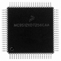
MC9S12XDT256CAA Freescale Semiconductor, MC9S12XDT256CAA Datasheet - Page 841

MC9S12XDT256CAA
Manufacturer Part Number
MC9S12XDT256CAA
Description
IC MCU 256K FLASH 80-QFP
Manufacturer
Freescale Semiconductor
Series
HCS12r
Datasheet
1.MC9S12XD64CAA.pdf
(1348 pages)
Specifications of MC9S12XDT256CAA
Core Processor
HCS12X
Core Size
16-Bit
Speed
80MHz
Connectivity
CAN, EBI/EMI, I²C, IrDA, LIN, SCI, SPI
Peripherals
LVD, POR, PWM, WDT
Number Of I /o
59
Program Memory Size
256KB (256K x 8)
Program Memory Type
FLASH
Eeprom Size
4K x 8
Ram Size
16K x 8
Voltage - Supply (vcc/vdd)
2.35 V ~ 5.5 V
Data Converters
A/D 8x10b
Oscillator Type
External
Operating Temperature
-40°C ~ 85°C
Package / Case
80-QFP
Processor Series
S12XD
Core
HCS12
Data Bus Width
16 bit
Data Ram Size
16 KB
Interface Type
CAN/I2C/SCI/SPI
Maximum Clock Frequency
40 MHz
Number Of Programmable I/os
59
Number Of Timers
12
Maximum Operating Temperature
+ 85 C
Mounting Style
SMD/SMT
3rd Party Development Tools
EWHCS12
Development Tools By Supplier
EVB9S12XDP512E
Minimum Operating Temperature
- 40 C
On-chip Adc
8-ch x 10-bit
Lead Free Status / RoHS Status
Lead free / RoHS Compliant
Available stocks
Company
Part Number
Manufacturer
Quantity
Price
Company:
Part Number:
MC9S12XDT256CAA
Manufacturer:
Freescale Semiconductor
Quantity:
10 000
Company:
Part Number:
MC9S12XDT256CAAR
Manufacturer:
Freescale Semiconductor
Quantity:
10 000
- Current page: 841 of 1348
- Download datasheet (8Mb)
22.3.2.22 Port T Polarity Select Register (PPST)
Read: Anytime.
Write: Anytime.
This register selects whether a pull-down or a pull-up device is connected to the pin.
22.3.2.23 Port S Data Register (PTS)
Read: Anytime.
Write: Anytime.
Port S pins 7–4 are associated with the SPI0. The SPI0 pin configuration is determined by several status
bits in the SPI0 module. Refer to SPI section for details. When not used with the SPI0, these pins can be
used as general purpose I/O.
Port S bits 3–0 are associated with the SCI1 and SCI0. The SCI ports associated with transmit pins 3 and
1 are configured as outputs if the transmitter is enabled. The SCI ports associated with receive pins 2 and
0 are configured as inputs if the receiver is enabled. Refer to SCI section for details. When not used with
the SCI, these pins can be used as general purpose I/O.
If the data direction bits of the associated I/O pins are set to logic level “1”, a read returns the value of the
port register, otherwise the buffered pin input state is read.
Freescale Semiconductor
SCI/SPI
PPST[7:0]
Reset
Reset
Field
7–0
W
W
R
R
PPST7
PTS7
Pull Select Port T
0 A pull-up device is connected to the associated port T pin, if enabled by the associated bit in register PERT
1 A pull-down device is connected to the associated port T pin, if enabled by the associated bit in register PERT
SS0
0
0
7
7
and if the port is used as input.
and if the port is used as input.
PPST6
SCK0
PTS6
0
0
6
6
Figure 22-24. Port T Polarity Select Register (PPST)
Figure 22-25. Port S Data Register (PTS)
Table 22-26. PPST Field Descriptions
PPST5
MOSI0
MC9S12XDP512 Data Sheet, Rev. 2.21
PTS5
0
0
5
5
PPST4
MISO0
PTS4
0
0
4
4
Description
Chapter 22 DP512 Port Integration Module (S12XDP512PIMV2)
PPST3
TXD1
PTS3
0
0
3
3
PPST2
RXD1
PTS2
0
0
2
2
PPST1
TXD0
PTS1
0
0
1
1
PPST0
RXD0
PTS0
0
0
0
0
843
Related parts for MC9S12XDT256CAA
Image
Part Number
Description
Manufacturer
Datasheet
Request
R

Part Number:
Description:
16-BIT MICROPROCESSOR FAMILY
Manufacturer:
FREESCALE [Freescale Semiconductor, Inc]
Datasheet:
Part Number:
Description:
Manufacturer:
Freescale Semiconductor, Inc
Datasheet:
Part Number:
Description:
Manufacturer:
Freescale Semiconductor, Inc
Datasheet:
Part Number:
Description:
Manufacturer:
Freescale Semiconductor, Inc
Datasheet:
Part Number:
Description:
Manufacturer:
Freescale Semiconductor, Inc
Datasheet:
Part Number:
Description:
Manufacturer:
Freescale Semiconductor, Inc
Datasheet:
Part Number:
Description:
Manufacturer:
Freescale Semiconductor, Inc
Datasheet:
Part Number:
Description:
Manufacturer:
Freescale Semiconductor, Inc
Datasheet:
Part Number:
Description:
Manufacturer:
Freescale Semiconductor, Inc
Datasheet:
Part Number:
Description:
Manufacturer:
Freescale Semiconductor, Inc
Datasheet:
Part Number:
Description:
Manufacturer:
Freescale Semiconductor, Inc
Datasheet:
Part Number:
Description:
Manufacturer:
Freescale Semiconductor, Inc
Datasheet:
Part Number:
Description:
Manufacturer:
Freescale Semiconductor, Inc
Datasheet:
Part Number:
Description:
Manufacturer:
Freescale Semiconductor, Inc
Datasheet:
Part Number:
Description:
Manufacturer:
Freescale Semiconductor, Inc
Datasheet:


