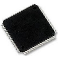
LCMXO2280C-5TN144C LATTICE SEMICONDUCTOR, LCMXO2280C-5TN144C Datasheet - Page 10

LCMXO2280C-5TN144C
Manufacturer Part Number
LCMXO2280C-5TN144C
Description
MACHXO PLD FLASH, SCRAM 1.8V, SMD
Manufacturer
LATTICE SEMICONDUCTOR
Series
MachXOr
Datasheet
1.LCMXO1200C-5TN144C.pdf
(244 pages)
Specifications of LCMXO2280C-5TN144C
Cpld Type
FLASH
No. Of Macrocells
1140
No. Of I/o's
113
Propagation Delay
3.6ns
Global Clock Setup Time
1.1ns
Frequency
600MHz
Supply Voltage Range
1.71V To 3.465V
Operating
RoHS Compliant
Available stocks
Company
Part Number
Manufacturer
Quantity
Price
Company:
Part Number:
LCMXO2280C-5TN144C
Manufacturer:
Lattice Semiconductor Corporation
Quantity:
10 000
Part Number:
LCMXO2280C-5TN144C
Manufacturer:
LATTICE/莱迪斯
Quantity:
20 000
- Current page: 10 of 244
- Download datasheet (9Mb)
www.latticesemi.com
© 2007 Lattice Semiconductor Corp. All Lattice trademarks, registered trademarks, patents, and disclaimers are as listed at www.latticesemi.com/legal. All other brand
or product names are trademarks or registered trademarks of their respective holders. The specifications and information herein are subject to change without notice.
February 2007
Architecture Overview
The MachXO family architecture contains an array of logic blocks surrounded by Programmable I/O (PIO). Some
devices in this family have sysCLOCK PLLs and blocks of sysMEM™ Embedded Block RAM (EBRs). Figures 2-1,
2-2, and 2-3 show the block diagrams of the various family members.
The logic blocks are arranged in a two-dimensional grid with rows and columns. The EBR blocks are arranged in a
column to the left of the logic array. The PIO cells are located at the periphery of the device, arranged into Banks.
The PIOs utilize a flexible I/O buffer referred to as a sysIO interface that supports operation with a variety of inter-
face standards. The blocks are connected with many vertical and horizontal routing channel resources. The place
and route software tool automatically allocates these routing resources.
There are two kinds of logic blocks, the Programmable Functional Unit (PFU) and the Programmable Functional
unit without RAM (PFF). The PFU contains the building blocks for logic, arithmetic, RAM, ROM, and register func-
tions. The PFF block contains building blocks for logic, arithmetic, ROM, and register functions. Both the PFU and
PFF blocks are optimized for flexibility, allowing complex designs to be implemented quickly and effectively. Logic
blocks are arranged in a two-dimensional array. Only one type of block is used per row.
In the MachXO family, the number of sysIO Banks varies by device. There are different types of I/O Buffers on dif-
ferent Banks. See the details in later sections of this document. The sysMEM EBRs are large, dedicated fast mem-
ory blocks; these blocks are found only in the larger devices. These blocks can be configured as RAM, ROM or
FIFO. FIFO support includes dedicated FIFO pointer and flag “hard” control logic to minimize LUT use.
The MachXO architecture provides up to two sysCLOCK™ Phase Locked Loop (PLL) blocks on larger devices.
These blocks are located at either end of the memory blocks. The PLLs have multiply, divide, and phase shifting
capabilities that are used to manage the frequency and phase relationships of the clocks.
Every device in the family has a JTAG Port that supports programming and configuration of the device as well as
access to the user logic. The MachXO devices are available for operation from 3.3V, 2.5V, 1.8V, and 1.2V power
supplies, providing easy integration into the overall system.
2-1
MachXO Family Data Sheet
Architecture
DS1002
Data Sheet DS1002
Architecture_01.4
Related parts for LCMXO2280C-5TN144C
Image
Part Number
Description
Manufacturer
Datasheet
Request
R
Part Number:
Description:
IC, CPLD, FLASH, 2280 MACROCELL FTBGA256
Manufacturer:
LATTICE SEMICONDUCTOR
Part Number:
Description:
CPLD MachXO Family 1140 Macro Cells 1.8V/2.5V/3.3V 324-Pin FTBGA Tray
Manufacturer:
LATTICE SEMICONDUCTOR
Datasheet:

Part Number:
Description:
Microcontroller Modules & Accessories MACHXO CNRL EVB
Manufacturer:
Lattice
Datasheet:

Part Number:
Description:
IC, CPLD, FLASH, 2280 MACROCELL, TQFP144
Manufacturer:
LATTICE SEMICONDUCTOR

Part Number:
Description:
MACHXO PLD FLASH, SCRAM 1.8V, SMD
Manufacturer:
LATTICE SEMICONDUCTOR
Datasheet:
Part Number:
Description:
CPLD MachXO Family 1140 Macro Cells 1.8V/2.5V/3.3V 256-Pin FTBGA Tray
Manufacturer:
LATTICE SEMICONDUCTOR
Datasheet:
Part Number:
Description:
CPLD MachXO Family 1140 Macro Cells 1.8V/2.5V/3.3V 324-Pin FTBGA Tray
Manufacturer:
LATTICE SEMICONDUCTOR
Datasheet:
Part Number:
Description:
CPLD MachXO Family 1140 Macro Cells 1.8V/2.5V/3.3V 100-Pin TQFP Tray
Manufacturer:
LATTICE SEMICONDUCTOR
Datasheet:
Part Number:
Description:
ISPLSI2032-80LT44Lattice Semiconductor [In-System Programmable High Density PLD]
Manufacturer:
Lattice Semiconductor Corp.
Datasheet:
Part Number:
Description:
IC PROGRAMMED LATTICE GAL 16V8
Manufacturer:
Lattice Semiconductor Corp.
Datasheet:
Part Number:
Description:
357-036-542-201 CARDEDGE 36POS DL .156 BLK LOPRO
Manufacturer:
Lattice Semiconductor Corp.
Datasheet:
Part Number:
Description:
357-036-542-201 CARDEDGE 36POS DL .156 BLK LOPRO
Manufacturer:
Lattice Semiconductor Corp.
Datasheet:
Part Number:
Description:
357-036-542-201 CARDEDGE 36POS DL .156 BLK LOPRO
Manufacturer:
Lattice Semiconductor Corp.
Datasheet:
Part Number:
Description:
357-036-542-201 CARDEDGE 36POS DL .156 BLK LOPRO
Manufacturer:
Lattice Semiconductor Corp.
Datasheet:


