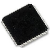
LCMXO2280C-5TN144C LATTICE SEMICONDUCTOR, LCMXO2280C-5TN144C Datasheet - Page 107

LCMXO2280C-5TN144C
Manufacturer Part Number
LCMXO2280C-5TN144C
Description
MACHXO PLD FLASH, SCRAM 1.8V, SMD
Manufacturer
LATTICE SEMICONDUCTOR
Series
MachXOr
Datasheet
1.LCMXO1200C-5TN144C.pdf
(244 pages)
Specifications of LCMXO2280C-5TN144C
Cpld Type
FLASH
No. Of Macrocells
1140
No. Of I/o's
113
Propagation Delay
3.6ns
Global Clock Setup Time
1.1ns
Frequency
600MHz
Supply Voltage Range
1.71V To 3.465V
Operating
RoHS Compliant
Available stocks
Company
Part Number
Manufacturer
Quantity
Price
Company:
Part Number:
LCMXO2280C-5TN144C
Manufacturer:
Lattice Semiconductor Corporation
Quantity:
10 000
Part Number:
LCMXO2280C-5TN144C
Manufacturer:
LATTICE/莱迪斯
Quantity:
20 000
- Current page: 107 of 244
- Download datasheet (9Mb)
Lattice Semiconductor
V
Each bank has a separate V
such as LVTTL, LVCMOS and PCI. LVTTL, LVCMOS3.3, LVCMOS2.5 and LVCMOS1.2 also have fixed threshold
options allowing them to be placed in any bank and is independent of bank V
bank determines the ratioed input standards that can be supported in that bank. It is also used to power the differ-
ential output drivers.
The V
and Bank5 for MachXO1200 and MachXO2280 devices). Therefore, the threshold of the JTAG pins is determined
by the V
V
In addition to the bank V
that powers the differential and referenced input buffers. V
headroom to satisfy the common-mode range requirements of these drivers and input buffers.
Mixed Voltage Support in a Bank
The MachXO sysIO buffer is connected to three parallel ratioed input buffers. These three parallel buffers are con-
nected to V
for 3.3V (V
by-pin basis, rather than being tracked with V
and is independent of the bank V
and 3.3V ratioed input buffers with fixed thresholds, as well as 2.5V ratioed inputs with tracking thresholds.
Prior to device configuration, the ratioed input thresholds always track the bank V
after configuration. Output standards within a bank are always set by V
that the user can mix in the same bank.
Table 8-2. Mixed Voltage Support
CCIO
CCAUX
V
1.2V
1.5V
1.8V
2.5V
3.3V
CCIO
CCIO
(1.2V/1.5V/1.8V/2.5V/3.3V)
CCIO
(3.3V)
CCAUX
of one of the banks is also used to power the JTAG pins (Bank1 for MachXO256, Bank2 for MachXO640
CCIO
of the JTAG bank.
1.2V
Yes
Yes
Yes
Yes
Yes
, V
) and 1.2V (V
CCAUX
1.5V
CCIO
Yes
and to V
Input sysIO Standards
CCIO
supplies, devices have a V
CC
) inputs. This allows the input threshold for ratioed buffers to be assigned on a pin-
CC
CCIO
supply that powers the single-ended output drivers and the ratioed input buffers
1.8V
Yes
, giving support for thresholds that track with V
voltage. For example, if the bank V
2.5V
CCIO
Yes
Yes
Yes
Yes
Yes
. This option is available for all 1.2V, 2.5V and 3.3V ratioed inputs
3.3V
Yes
Yes
Yes
Yes
Yes
8-4
CC
CCAUX
core logic power supply, and a V
1.2V
is required because V
Yes
CCIO
CCIO
. Table 8-2 shows the sysIO standards
1.5V
CCIO
Yes
Output sysIO Standards
MachXO sysIO Usage Guide
is 1.8V, it is possible to have 1.2V
. The V
CCIO
CCIO
. This option only takes effect
1.8V
Yes
, as well as fixed thresholds
CCIO
CC
does not have enough
CCAUX
voltage applied to the
2.5V
Yes
auxiliary supply
3.3V
Yes
Related parts for LCMXO2280C-5TN144C
Image
Part Number
Description
Manufacturer
Datasheet
Request
R
Part Number:
Description:
IC, CPLD, FLASH, 2280 MACROCELL FTBGA256
Manufacturer:
LATTICE SEMICONDUCTOR
Part Number:
Description:
CPLD MachXO Family 1140 Macro Cells 1.8V/2.5V/3.3V 324-Pin FTBGA Tray
Manufacturer:
LATTICE SEMICONDUCTOR
Datasheet:

Part Number:
Description:
Microcontroller Modules & Accessories MACHXO CNRL EVB
Manufacturer:
Lattice
Datasheet:

Part Number:
Description:
IC, CPLD, FLASH, 2280 MACROCELL, TQFP144
Manufacturer:
LATTICE SEMICONDUCTOR

Part Number:
Description:
MACHXO PLD FLASH, SCRAM 1.8V, SMD
Manufacturer:
LATTICE SEMICONDUCTOR
Datasheet:
Part Number:
Description:
CPLD MachXO Family 1140 Macro Cells 1.8V/2.5V/3.3V 256-Pin FTBGA Tray
Manufacturer:
LATTICE SEMICONDUCTOR
Datasheet:
Part Number:
Description:
CPLD MachXO Family 1140 Macro Cells 1.8V/2.5V/3.3V 324-Pin FTBGA Tray
Manufacturer:
LATTICE SEMICONDUCTOR
Datasheet:
Part Number:
Description:
CPLD MachXO Family 1140 Macro Cells 1.8V/2.5V/3.3V 100-Pin TQFP Tray
Manufacturer:
LATTICE SEMICONDUCTOR
Datasheet:
Part Number:
Description:
ISPLSI2032-80LT44Lattice Semiconductor [In-System Programmable High Density PLD]
Manufacturer:
Lattice Semiconductor Corp.
Datasheet:
Part Number:
Description:
IC PROGRAMMED LATTICE GAL 16V8
Manufacturer:
Lattice Semiconductor Corp.
Datasheet:
Part Number:
Description:
357-036-542-201 CARDEDGE 36POS DL .156 BLK LOPRO
Manufacturer:
Lattice Semiconductor Corp.
Datasheet:
Part Number:
Description:
357-036-542-201 CARDEDGE 36POS DL .156 BLK LOPRO
Manufacturer:
Lattice Semiconductor Corp.
Datasheet:
Part Number:
Description:
357-036-542-201 CARDEDGE 36POS DL .156 BLK LOPRO
Manufacturer:
Lattice Semiconductor Corp.
Datasheet:
Part Number:
Description:
357-036-542-201 CARDEDGE 36POS DL .156 BLK LOPRO
Manufacturer:
Lattice Semiconductor Corp.
Datasheet:


