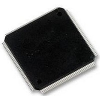
LCMXO2280C-5TN144C LATTICE SEMICONDUCTOR, LCMXO2280C-5TN144C Datasheet - Page 224

LCMXO2280C-5TN144C
Manufacturer Part Number
LCMXO2280C-5TN144C
Description
MACHXO PLD FLASH, SCRAM 1.8V, SMD
Manufacturer
LATTICE SEMICONDUCTOR
Series
MachXOr
Datasheet
1.LCMXO1200C-5TN144C.pdf
(244 pages)
Specifications of LCMXO2280C-5TN144C
Cpld Type
FLASH
No. Of Macrocells
1140
No. Of I/o's
113
Propagation Delay
3.6ns
Global Clock Setup Time
1.1ns
Frequency
600MHz
Supply Voltage Range
1.71V To 3.465V
Operating
RoHS Compliant
Available stocks
Company
Part Number
Manufacturer
Quantity
Price
Company:
Part Number:
LCMXO2280C-5TN144C
Manufacturer:
Lattice Semiconductor Corporation
Quantity:
10 000
Part Number:
LCMXO2280C-5TN144C
Manufacturer:
LATTICE/莱迪斯
Quantity:
20 000
- Current page: 224 of 244
- Download datasheet (9Mb)
September 2010
Introduction
As Ball Grid Array (BGA) packages become increasingly popular and become more populated across the array
with higher pin count and smaller pitch, it is important to understand how they are affected by various board layout
techniques. This document provides a brief overview of PCB layout considerations when working with BGA pack-
ages. It outlines some of the most common problems and provides tips for avoiding them at the design stage. A key
challenge of adopting fine-pitch (0.8 mm or less) BGA packages is the design of a route fanout pattern that maxi-
mizes I/O utilization while minimizing fabrication cost. This technical note provides an overview of PCB design
examples provided by Lattice Semiconductor.
For more information and design examples see the PCB Design Support page at the Lattice Semiconductor web
site (www.latticesemi.com/support/pcbdesignsupport.cfm).
BGA Board Layout Recommendations
All Lattice BGA packages have Solder Mask Defined (SMD) pads. In order to evenly balance the stress in the sol-
der joints, Lattice recommends PCB solder pads be SMD with dimensions as similar to the applicable BGA as pos-
sible. If Non Solder Mask Defined Pads (NSMD) are used, the optimum pad dimensions will result in an equivalent
surface contact area on the PCB as on the BGA component.
Table 14-1. Lattice Semiconductor SMD/NSMD Pad Recommendations
© 2010 Lattice Semiconductor Corp. All Lattice trademarks, registered trademarks, patents, and disclaimers are as listed at www.latticesemi.com/legal. All other brand
or product names are trademarks or registered trademarks of their respective holders. The specifications and information herein are subject to change without notice.
www.latticesemi.com
Nominal BGA
package pad
opening diameter
(mm) - SMD
PCB Solder Mask Defined (SMD) Pad Recommendations
Optimum solder
mask opening
PCB Non Solder Mask Defined (NSMD) Pad Recommendations
Optimum solder
land diameter
1. These Lattice-recommended PCB design values will result in optimum Board Level Reliability (BLR) performance for each corresponding
2. ispMACH 4000, MachXO, LatticeXP2.
3. LatticeECP3.
package. Those who use PCB design values which deviate from these recommendations should understand that the BLR performance may
be reduced.
Ball Pitch
0.4 mm
64, 132
ucBGA
0.20
0.22
0.17
Ball Pitch
100, 132,
0.5 mm
csBGA
56, 64,
0.27
0.30
0.25
144
Ball Pitch
49, 100,
0.8 mm
caBGA
0.40
0.40
0.35
256
PCB Layout Recommendations
100 fpBGA,
(Option 1
256 ftBGA
14-1
0.40
0.40
0.35
2
)
256, 388, 416, 484, 516,
256 ftBGA (Option 2
324 ftBGA, 144, 208,
672, 676, 900, 1152,
1156 fpBGA
Ball Pitch
1.0 mm
0.45
0.45
0.40
for BGA Packages
1
3
),
1704 Organic
1020, 1152,
Technical Note TN1074
fcBGA
0.50
0.50
0.45
tn1074_01.9
352 SBGA
Ball Pitch
256, 320,
1.27 mm
272, 388
PBGA,
0.60
0.60
0.55
Related parts for LCMXO2280C-5TN144C
Image
Part Number
Description
Manufacturer
Datasheet
Request
R
Part Number:
Description:
IC, CPLD, FLASH, 2280 MACROCELL FTBGA256
Manufacturer:
LATTICE SEMICONDUCTOR
Part Number:
Description:
CPLD MachXO Family 1140 Macro Cells 1.8V/2.5V/3.3V 324-Pin FTBGA Tray
Manufacturer:
LATTICE SEMICONDUCTOR
Datasheet:

Part Number:
Description:
Microcontroller Modules & Accessories MACHXO CNRL EVB
Manufacturer:
Lattice
Datasheet:

Part Number:
Description:
IC, CPLD, FLASH, 2280 MACROCELL, TQFP144
Manufacturer:
LATTICE SEMICONDUCTOR

Part Number:
Description:
MACHXO PLD FLASH, SCRAM 1.8V, SMD
Manufacturer:
LATTICE SEMICONDUCTOR
Datasheet:
Part Number:
Description:
CPLD MachXO Family 1140 Macro Cells 1.8V/2.5V/3.3V 256-Pin FTBGA Tray
Manufacturer:
LATTICE SEMICONDUCTOR
Datasheet:
Part Number:
Description:
CPLD MachXO Family 1140 Macro Cells 1.8V/2.5V/3.3V 324-Pin FTBGA Tray
Manufacturer:
LATTICE SEMICONDUCTOR
Datasheet:
Part Number:
Description:
CPLD MachXO Family 1140 Macro Cells 1.8V/2.5V/3.3V 100-Pin TQFP Tray
Manufacturer:
LATTICE SEMICONDUCTOR
Datasheet:
Part Number:
Description:
ISPLSI2032-80LT44Lattice Semiconductor [In-System Programmable High Density PLD]
Manufacturer:
Lattice Semiconductor Corp.
Datasheet:
Part Number:
Description:
IC PROGRAMMED LATTICE GAL 16V8
Manufacturer:
Lattice Semiconductor Corp.
Datasheet:
Part Number:
Description:
357-036-542-201 CARDEDGE 36POS DL .156 BLK LOPRO
Manufacturer:
Lattice Semiconductor Corp.
Datasheet:
Part Number:
Description:
357-036-542-201 CARDEDGE 36POS DL .156 BLK LOPRO
Manufacturer:
Lattice Semiconductor Corp.
Datasheet:
Part Number:
Description:
357-036-542-201 CARDEDGE 36POS DL .156 BLK LOPRO
Manufacturer:
Lattice Semiconductor Corp.
Datasheet:
Part Number:
Description:
357-036-542-201 CARDEDGE 36POS DL .156 BLK LOPRO
Manufacturer:
Lattice Semiconductor Corp.
Datasheet:


